Liquid crystal display device having array substrate of color filter on thin film transistor structure and manufacturing method thereof

a thin film transistor and array substrate technology, applied in the field of liquid crystal display devices, can solve the problems of deteriorating the image quality of the lcd device, achieve the effects of improving the manufacturing yield, simplifying the manufacturing process, and high aperture ratio

Inactive Publication Date: 2005-03-29
LG DISPLAY CO LTD
View PDF5 Cites 48 Cited by
  • Summary
  • Abstract
  • Description
  • Claims
  • Application Information

AI Technical Summary

Benefits of technology

Another object of the present invention is to provide an array substrate for a liquid crystal display device, which provides a high aperture ratio.
Another object of the present invention is to provide a method of forming an array substrate for a liquid crystal display device, which simplifies a manufacturing process and increases a manufacturing yield.

Problems solved by technology

Moreover, if there are errors in the aligning margin of the black matrix 6, the light leakage occurs in the open spaces A and B, and deteriorates the image quality of the LCD device.

Method used


Image

  • Liquid crystal display device having array substrate of color filter on thin film transistor structure and manufacturing method thereof
  • Liquid crystal display device having array substrate of color filter on thin film transistor structure and manufacturing method thereof
  • Liquid crystal display device having array substrate of color filter on thin film transistor structure and manufacturing method thereof

Examples


Embodiment Construction

Reference will now be made in detail to the illustrated embodiments of the present invention, examples of which are illustrated in the accompanying drawings. Wherever possible, the same reference numbers will be used throughout the drawings to refer to the same or like parts.

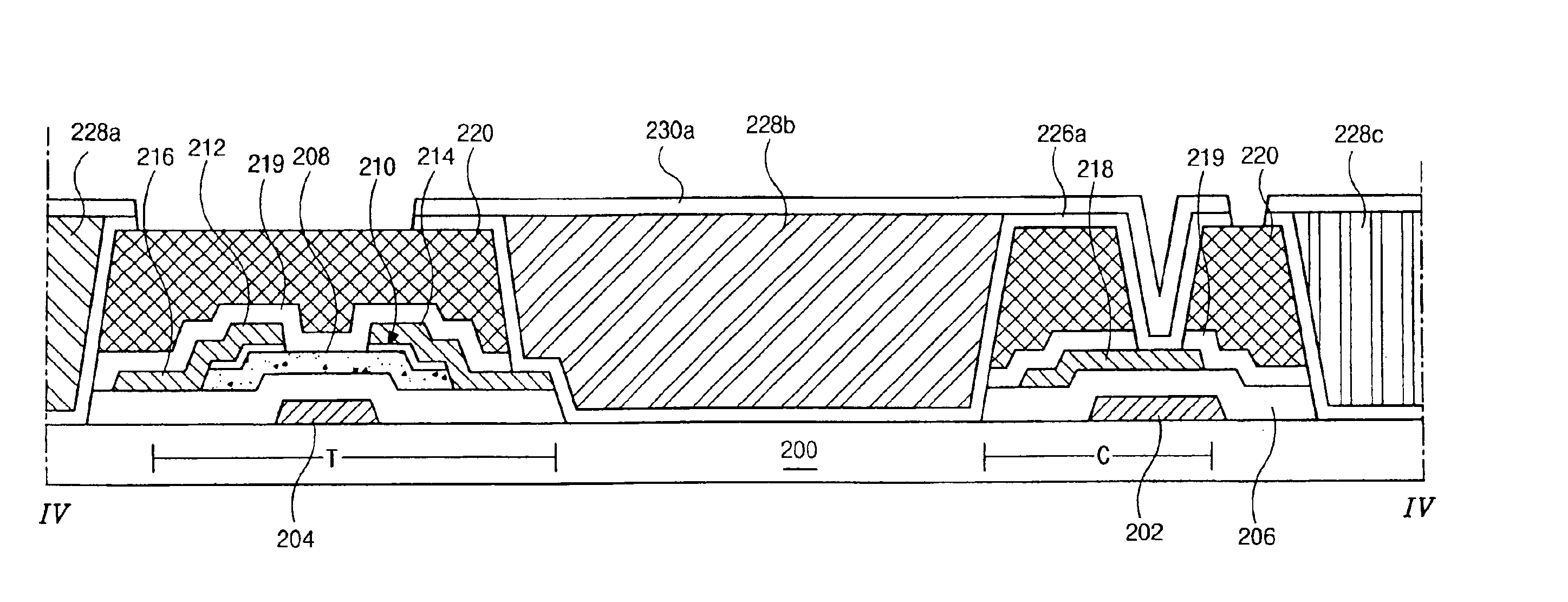
FIG. 3 is a partial schematic plane view of an array substrate having a color filter on thin film transistor structure according to the present invention.

As shown in FIG. 3, an array substrate 100 includes a plurality of gate lines 102 disposed in a transverse direction and a plurality of data lines 116 disposed in a longitudinal direction. The plurality of gate lines 102 and the plurality of data lines 116 cross one another defining a pixel region P. A thin film transistor T is formed at each crossing portion of the gate line 102 and the data line 116. The thin film transistor T includes a gate electrode 104, an active layer 108, a source electrode 112, and a drain electrode 114. In the pixel regions P defined ...


PUM

PropertyMeasurementUnit
insulatingaaaaaaaaaa
transparentaaaaaaaaaa
electric fieldsaaaaaaaaaa

Abstract

A liquid crystal display device having an array substrate of a color filter on a thin film transistor structure and a manufacturing method thereof are disclosed in the present invention. The liquid crystal display device having an array substrate includes an array substrate, a plurality of gate lines and data lines over the substrate, the gate and data lines defining a pixel region, a thin film transistor formed at each crossing region of the gate lines and the data lines, the thin film transistor including a gate electrode, an active layer, a source electrode, and a drain electrode, a black matrix over the thin film transistor, exposing a portion of the drain electrode, a first pixel electrode at the pixel region, contacting the exposed portion of the drain electrode, a color filter on the first pixel electrode at the pixel region, and a second pixel electrode on the color filter, directly contacting the first pixel electrode.

Description

This application claims the benefit of the Korean Application No. P2002-036998 filed on Jun. 28, 2002, which is hereby incorporated by reference.BACKGROUND OF THE INVENTION1. Field of the InventionThe present invention relates to a liquid crystal display device, and more particularly, to a liquid crystal display device having an array substrate of a color filter on thin film transistor structure and a manufacturing method thereof. Although the present invention is suitable for a wide scope of applications, it is particularly suitable for increasing an aperture ratio and simplifying the fabrication process.2. Discussion of the Related ArtIn general, since flat panel display devices are thin, light weight, and have low power consumption, they have been used for displays of portable devices. Among the various types of flat panel display devices, liquid crystal display (LCD) devices are widely used for laptop computers and desktop computer monitors because of their superiority in resolu...

Claims


Application Information

Patent Timeline
Patent Type & Authority Patents(United States)
IPC IPC(8): G02F1/13G02F1/1362G02B5/20G02F1/1335G02F1/1368
CPCG02F1/136227G02F1/136209G02F2001/136222G02F1/136222G02F1/1335
Inventor CHANG, YOUN-GYOUNGPARK, SEUNG-RYUL
Owner LG DISPLAY CO LTD
Why Eureka
Try Eureka