Method and apparatus for broadband optical end point determination for in-situ film thickness measurement

a technology of optical end point and in-situ film thickness measurement, which is applied in the direction of measuring devices, instruments, and using optical means, can solve the problems of insufficient efficiency of epd methods based on detecting the transition from one layer to the next underlying layer, insufficient method, and high approximation sensitivity, so as to reduce the number of parameters

Inactive Publication Date: 2005-04-05
LAM RES CORP
View PDF3 Cites 3 Cited by
  • Summary
  • Abstract
  • Description
  • Claims
  • Application Information

AI Technical Summary

Benefits of technology

Broadly speaking, the present invention fills these needs by providing a method and system that considers the differences between multiple shots to discard reflectance spectra contribution that does not change from shot to shot to reduce the nu

Problems solved by technology

Therefore, EPD methods based on detecting the transition from one layer to the next underlying layer are not efficient enough when dealing with these thin transparent films encountered during upper layer removal processes.
However, when the spectrometer measurement band is 300 nanometers-700 nanometers, this method is inadequate for measuring the thickness of a layer that is less then about 300-600 of a nanometer (nm).
The multiparametric model disadvantages include high sensitivity of the approximation to precise values of introduced parameters and exis

Method used


Image

  • Method and apparatus for broadband optical end point determination for in-situ film thickness measurement
  • Method and apparatus for broadband optical end point determination for in-situ film thickness measurement
  • Method and apparatus for broadband optical end point determination for in-situ film thickness measurement

Examples


Embodiment Construction

Several exemplary embodiments of the invention will now be described in detail with reference to the accompanying drawings. It should be appreciated that like numerals represent like structures.

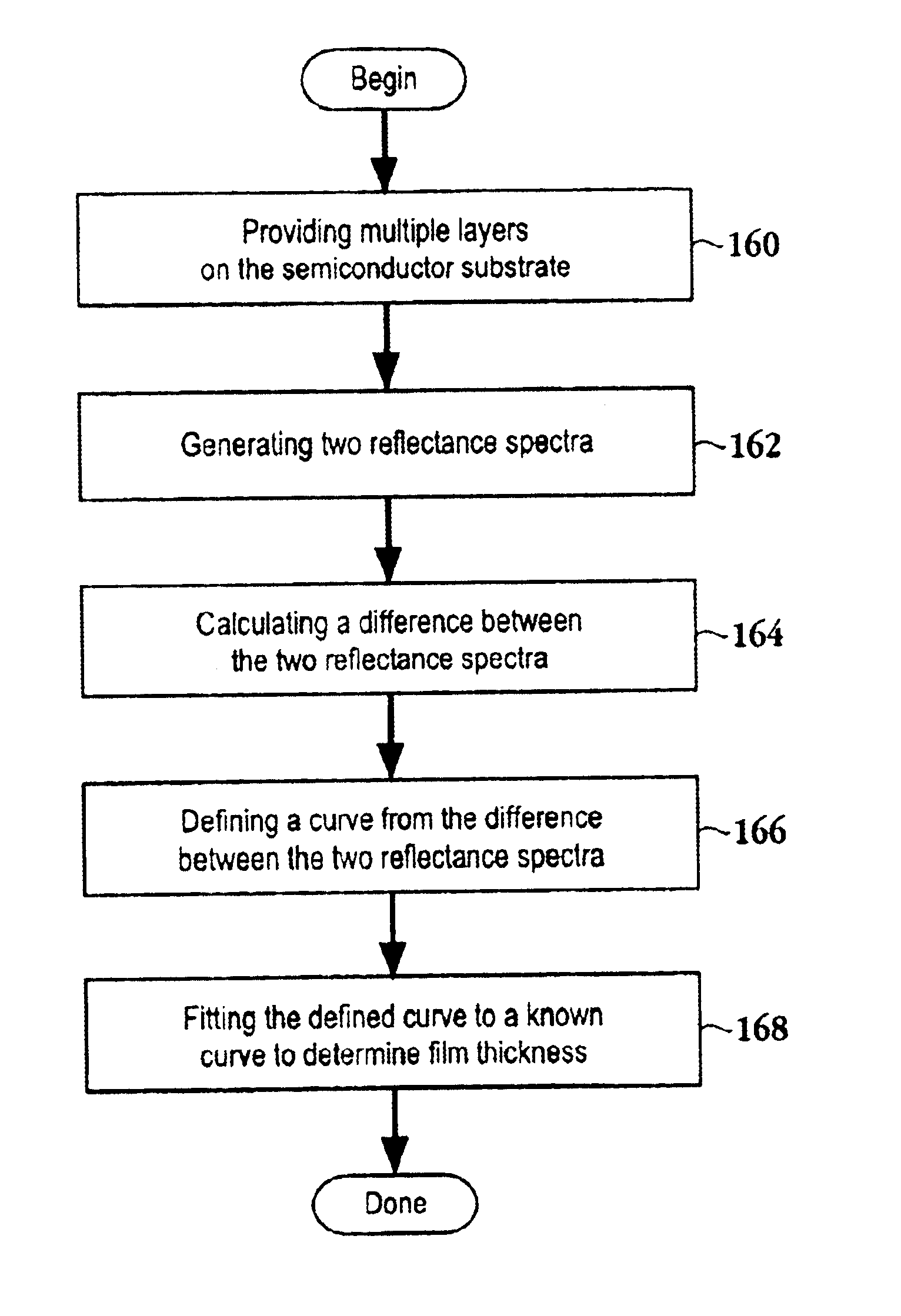
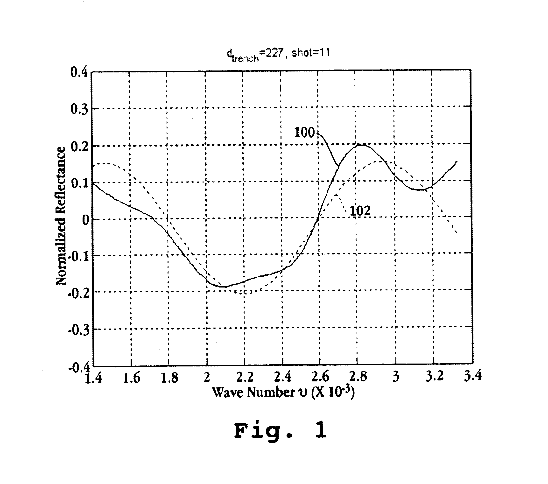
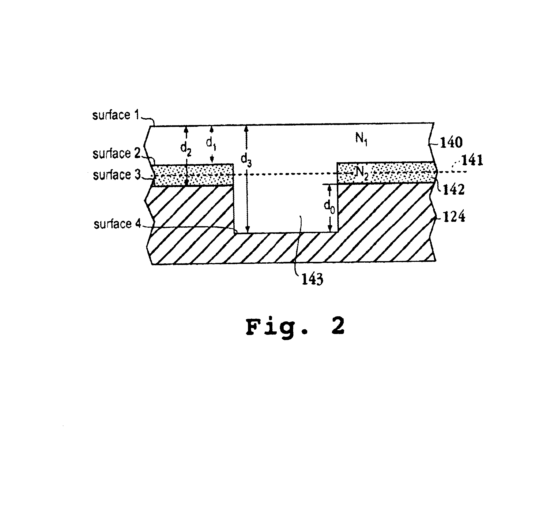
The embodiments described herein propose a method and apparatus which allows for the reliable measurement the thickness of thin films, which in turn can be used for endpoint determination. It should be appreciated that while the embodiments described herein allow for the measurement of films having a thickness that is less than about 600 nanometers (nm), the embodiments are also effective for measuring films having a thickness of 600 nm or more. In one embodiment, the method and apparatus use the dominant reflectance of silicon to determine a trench depth in a silicon substrate as the upper layers are planarized or etched.

Processes, such as chemical mechanical planarization (CMP) or etch processes deal not with a single spectrum but with series of spectra corresponding to the decreasing thick...


PUM


Abstract

A method for determining a film thickness in a semiconductor substrate is provided. The method initiates with providing multiple layers on the semiconductor substrate. Then, two reflectance spectra are generated where each of the two reflectance spectra are associated with different time periods while an upper layer is being removed. Next, a difference between the two reflectance spectra is calculated. Then, a curve is defined from the difference between the two reflectance spectra. Next, the defined curve is fitted by a known parametric function to determine the film thickness. An endpoint detector and a CMP system are also provided.

Description

BACKGROUND OF THE INVENTIONThe invention relates generally to semiconductor fabrication and more specifically to in-situ film thickness measurement for thin films deposited on a semiconductor substrate utilizing broad band spectrometry.During semiconductor fabrication there are multiple steps where an underlying substrate is subjected to the formation and removal of various layers. The small feature sizes and tight surface planarity requirements, combined with the constant quest to increase throughput, makes it highly desirable to stop the process when the correct thickness has been achieved, i.e., when an endpoint has been obtained for the process step.Present optical end point detection (EPD) methods make use of Broad Band Visible Spectra Spectrometry. The light of a lamp flash, i.e., shot, is returned from a wafer while an upper film is removed through a chemical mechanical planarization (CMP) or etch process. The light spectrum returned is measured for each shot and analyzed acc...

Claims


Application Information

Patent Timeline
IPC IPC(8): G01B11/06
CPCG01B11/0625
Inventor KATZ, VLADIMIRMITCHELL, BELLA
Owner LAM RES CORP
Why Eureka
Try Eureka