Reset control system and method

a control system and control method technology, applied in the field of reset control systems and methods, can solve the problems of system not being completely reset, no correct debugging can be performed, etc., and achieve the effect of avoiding undesirable reset by external reset signals

Inactive Publication Date: 2005-04-05
FUJITSU LTD
View PDF7 Cites 27 Cited by
  • Summary
  • Abstract
  • Description
  • Claims
  • Application Information

AI Technical Summary

Benefits of technology

In another characteristic feature of the present invention, when the emulator is in operation, the external reset signal is masked and invalidated. Even when the external reset signal is undesirably input during debug, the external reset signal can be invalidated, and the central processing section or the peripheral control section can hold internal data during debug without being initialized. Hence, undesirable reset by the external reset signal can be avoided.
When the synchronization processing section is provided, any time lag for reset cancel due to a difference in internal circuit between the central processing section and the peripheral control section is adjusted, and the central processing section and the peripheral control section are synchronously activated after reset operation. For this reason, one chip that has been activated earlier can be prevented from accessing the other chip that has not been activated yet.

Problems solved by technology

No correct debug can be performed unless both chips are initialized.
Hence, the system cannot be totally reset.

Method used


Image

  • Reset control system and method
  • Reset control system and method
  • Reset control system and method

Examples


first embodiment

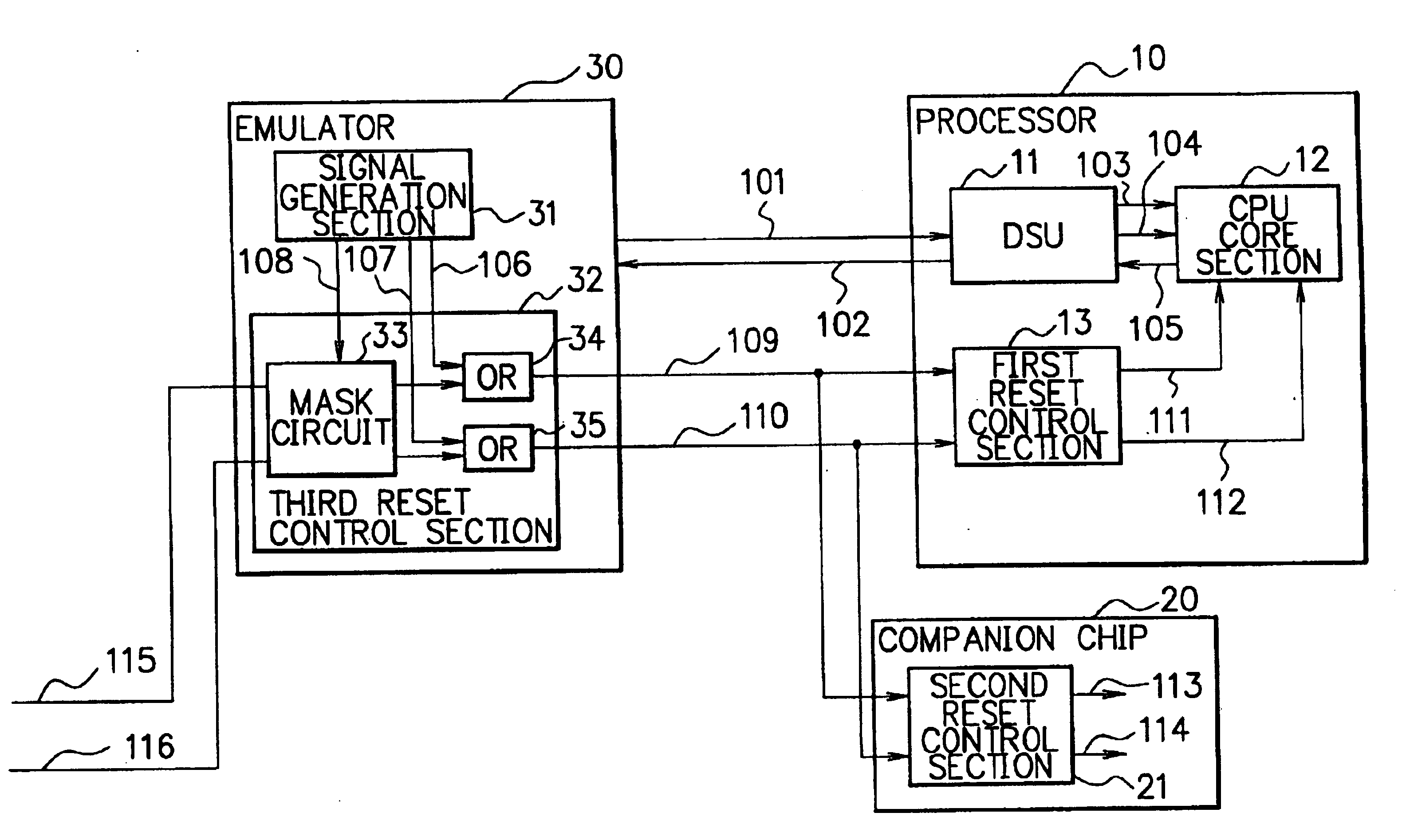
FIG. 4 is a block diagram showing the construction of a system using a reset control system according to the present invention. This system includes a processor and a companion chip connected to the processor.

In this embodiment, as reset types, for example, power-on reset and hard reset will be described. Power-on reset is reset when powering on, which initializes the whole of the internal states of the processor and the companion chip. Contrastingly, hard reset partially initializes the internal states of the processor and the companion chip.

Referring to FIG. 4, reference numeral 10 denotes a processor; 20 denotes a companion chip; and 30 denotes an emulator. The processor 10 has a DSU 11, a CPU core section 12, and a first reset control section 13. The DSU 11 has an interface to the emulator 30 to receive a debug command 101 transmitted from the emulator 30 and transmit an execution result 102 to the emulator 30. When receiving the debug command 101 transmitted from the emulator 3...

second embodiment

the present invention will be described next.

FIG. 5 is a block diagram showing the construction of a system using a reset control system according to the second embodiment. In FIG. 5, the same reference numerals as in FIG. 4 denote the same blocks as in FIG. 4, respectively, and a detailed description thereof will be omitted.

In the first embodiment shown in FIG. 4, the reset control section for generating a system reset signal is provided in the emulator 30. In the second embodiment, however, the corresponding reset control section for generating a system reset signal is provided in a processor 40.

Additionally, in the first embodiment shown in FIG. 4, the first reset control section 13 is provided in the processor 10, and the second reset control section 21 is provided in the companion chip 20. In the second embodiment, however, neither of the first and second reset control sections is provided.

Referring to FIG. 5, reference numeral 40 denotes a processor; 50 denotes a companion chi...

third embodiment

the present invention will be described next.

FIG. 6 is a block diagram showing the construction of a system using a reset control system according to the third embodiment. In FIG. 6, the same reference numerals as in FIGS. 4 and 5 denote the same blocks as in FIGS. 4 and 5, respectively, and a detailed description thereof will be omitted.

Referring to FIG. 6, reference numeral 40′ denotes a processor which includes a DSU 41′, a CPU core section 12, and a reset control section 42′. The DSU 41′ has an interface to an emulator 60 to receive a debug command 101 transmitted from the emulator 60 and transmit an execution result 102 to the emulator 60. When receiving the debug command 101 transmitted from the emulator 60, the DSU 41′ outputs a reset selection signal 123 and a debug mode signal 103 to make the processor 40′ transit from the user mode to the debug mode. The DSU 41′ also decodes the received debug command 101.

If the decoding result reveals that the debug command 101 received f...


PUM


Abstract

An OR circuit (34, 35) OR-operates an emulator reset signal (106, 107) based on a reset instruction from an emulator (30) and an external reset signal (115, 116) supplied from an external reset generation circuit. The OR operation result is distributed and supplied to a processor (10) and a companion chip (20) as a system reset signal (109, 110), thereby initializing both chips of the processor (10) and the companion chip (20) in accordance with the reset the emulator (30).

Description

BACKGROUND OF THE INVENTION1. Field of the InventionThe present invention relates to reset control systems and methods, particularly to reset control schemes for systems provided with a processor having a debug support function and a companion chip connected to the processor.2. Description of the Related ArtIn a conventional system using a processor, the processor incorporates a DSU (Debug Support Unit) having a debug support function for software debug during program development or hardware debug during system development. An external emulator prepared for debug is connected to the DSU, and a debug command is supplied from the external emulator to the DSU, thereby performing system debug.FIG. 1 is a block diagram showing a conventional system having a processor and an emulator.Referring to FIG. 1, reference numeral 401 denotes an emulator for emulating debug processing; and 402 denotes a processor for performing various data processing operations. The processor 402 has a CPU core 4...

Claims


Application Information

Patent Timeline
Patent Type & Authority Patents(United States)
IPC IPC(8): G06F1/24G06F11/00G06F11/22G06F11/28
CPCG06F11/3652
Inventor IINO, HIDEYUKIUTSUMI, HIROYUKIHIROSE, YOSHIORYU, KEN
Owner FUJITSU LTD
Why Eureka
Try Eureka