Method and apparatus for routing an integrated circuit

a technology of integrated circuits and routing methods, applied in the field of circuit design, can solve the problems of limited spatial resources available in integrated circuits, tradeoffs between circuit complexity and design time, and the practical limit on the number of transistors on the integrated circuit di

Inactive Publication Date: 2005-04-05
SYNOPSYS INC
View PDF16 Cites 24 Cited by
  • Summary
  • Abstract
  • Description
  • Claims
  • Application Information

AI Technical Summary

Problems solved by technology

Integrated circuits have a long history of growing in complexity and scale.
Limited spatial resources available in integrated circuits have ied to tradeoffs between circuit complexity and design time.
At times, integrated circuits have been constrained due to overall size of wafers and defect densities, resulting in a practical limit on the number of transistors on an integrated circuit die, and a corresponding limit on design complexity.
Analog circuit designers tend to face additional challenges when designing, placing and routing a circuit for fabrication as an integrated circuit.
For example, analog circuits are notoriously sensitive to noise, whereas digital circuits tend to exhibit robust behavior in the face of noise.
Moreover, conductors of all types, but particularly some analog circuit conductors are subject to electromigration problems, thus requiring a minimum height and width to the conductors.
Moreover, analog circuits operate as fast as current flows, typically without the benefit of a clock which allows for alignment of signals and margin for error in signal skew.
Thus, when an analog circuit includes a differential pair of signals, skew between the signals (such as due to conductor differences or routing differences) may result in improper operation.
An amplifier with two differential inputs having unreasonable skew may produce an unacceptable output (incorrect polarity and magnitude for example) due to comparison of two input signals which were skewed.
Moreover, transition of the output to an acceptable output may be slow due to slew rate limitations imposed by power supply conductors in a circuit.
Long signal conductors will likely have a direct effect on the response time a circuit exhibits, mismatched signal conductors will likely result in unacceptable performance, and inefficient routing may result in overly large (and therefore costly) integrated circuits.

Method used


Image

  • Method and apparatus for routing an integrated circuit
  • Method and apparatus for routing an integrated circuit
  • Method and apparatus for routing an integrated circuit

Examples


Embodiment Construction

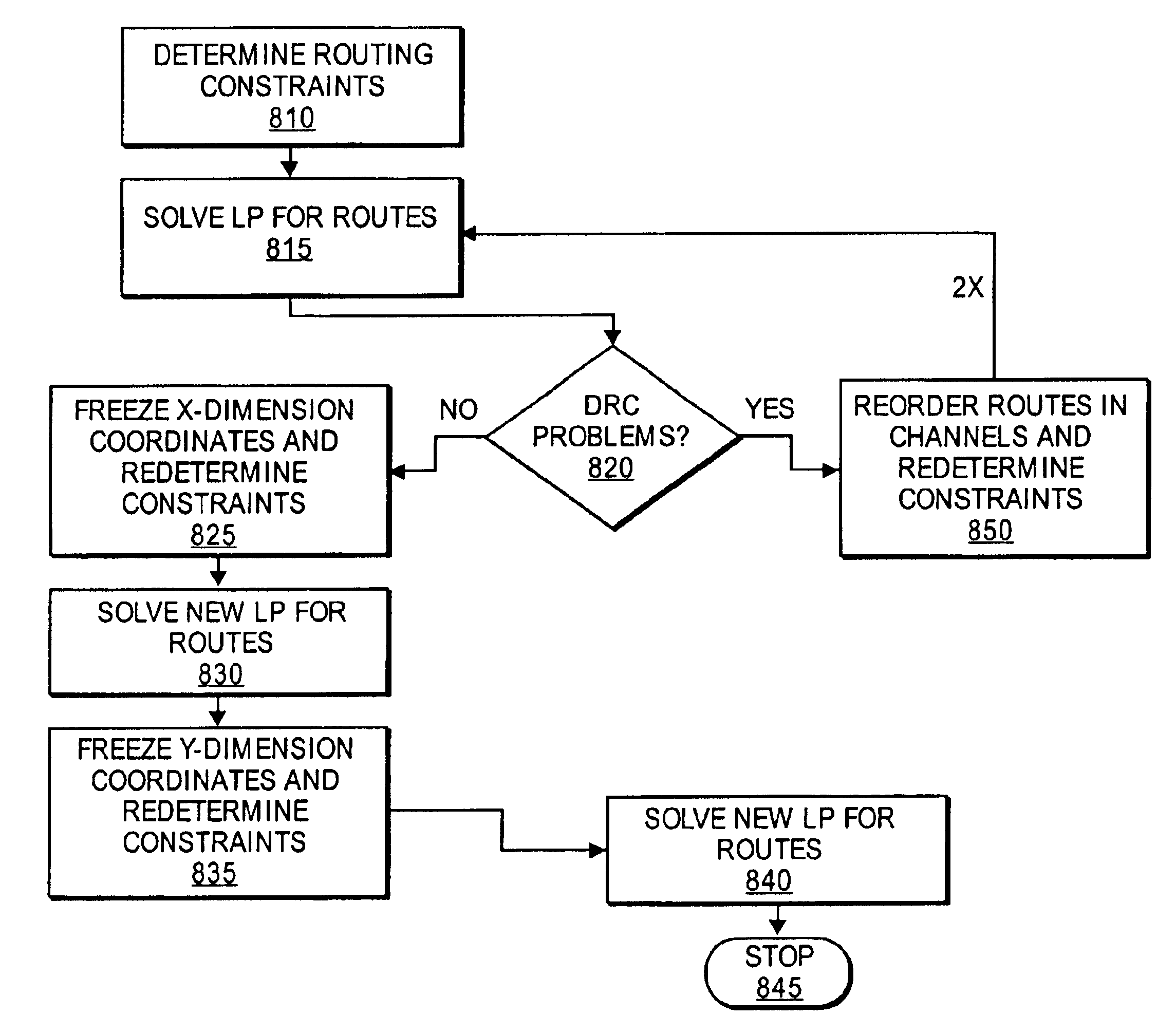
A method and apparatus for routing an integrated circuit is described. In the following description, for purposes of explanation, numerous specific details are set forth in order to provide a thorough understanding of the invention. It will be apparent, however, to one skilled in the art that the invention can be practiced without these specific details. In other instances, structures and devices are shown in block diagram form in order to avoid obscuring the invention.

Reference in the specification to “one embodiment” or “an embodiment” means that a particular feature, structure, or characteristic described in connection with the embodiment is included in at least one embodiment of the invention. The appearances of the phrase “in one embodiment” in various places in the specification are not necessarily all referring to the same embodiment, nor are separate or alternative embodiments mutually exclusive of other embodiments.

Introduction

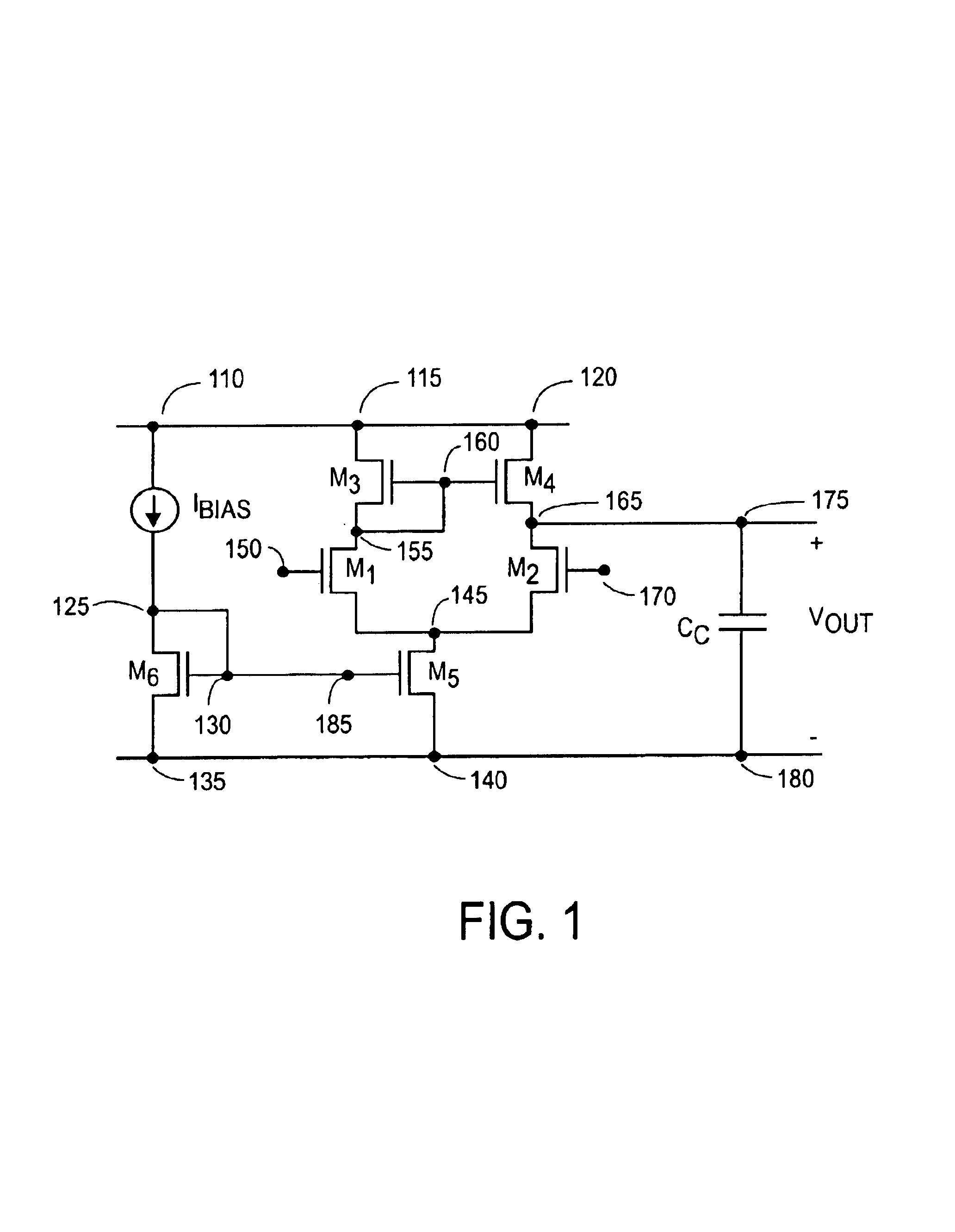
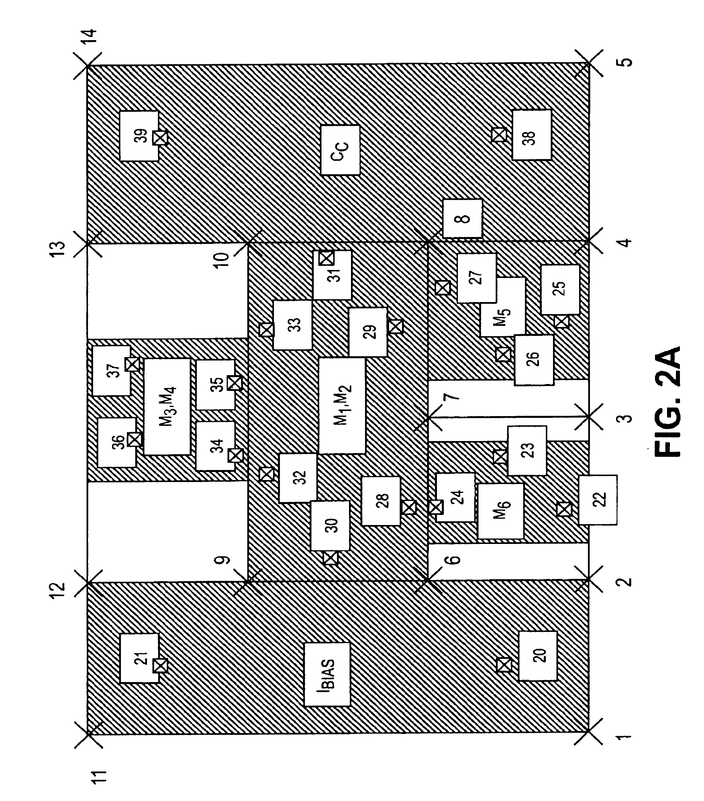
Ideally, a circuit designer may specify for a p...


PUM


Abstract

In one embodiment, the invention is a method. The method is a method of routing a circuit having a set of nets and a set of circuit elements specified as a slicing tree and a set of linear constraints. The method includes finding short paths for the set of nets based on a minimum-spanning-tree solution to a floorplan derived from the slicing tree for each net of the set of nets. The method also includes routing the nets as conductors within channels of the floorplan, the conductors having locations satisfying a set of linear constraints based on the solution of a linear optimization problem.

Description

BACKGROUND OF THE INVENTION1. Field of the InventionThe invention generally relates to circuit design and more specifically relates to automated routing of integrated circuits.2. Description of the Related ArtIntegrated circuits have a long history of growing in complexity and scale. While laying out the first inverter or current mirror may not have presented challenges, integrated circuits have grown exponentially in terms of transistors and other circuit elements. With this growth in circuit elements has come similar growth in interconnection between circuit elements. Limited spatial resources available in integrated circuits have ied to tradeoffs between circuit complexity and design time. At times, integrated circuits have been constrained due to overall size of wafers and defect densities, resulting in a practical limit on the number of transistors on an integrated circuit die, and a corresponding limit on design complexity. At other times, integrated circuits have been constra...

Claims


Application Information

Patent Timeline
Patent Type & Authority Patents(United States)
IPC IPC(8): G06F17/50
CPCG06F17/5077G06F30/394
Inventor HASSIBI, ARASHFONG, LUNGYINGBOYD, STEPHEN
Owner SYNOPSYS INC
Why Eureka
Try Eureka