CMOS imager with integrated non-volatile memory

Inactive Publication Date: 2005-04-12
MICRON TECH INC
View PDF19 Cites 125 Cited by
  • Summary
  • Abstract
  • Description
  • Claims
  • Application Information

AI Technical Summary

Benefits of technology

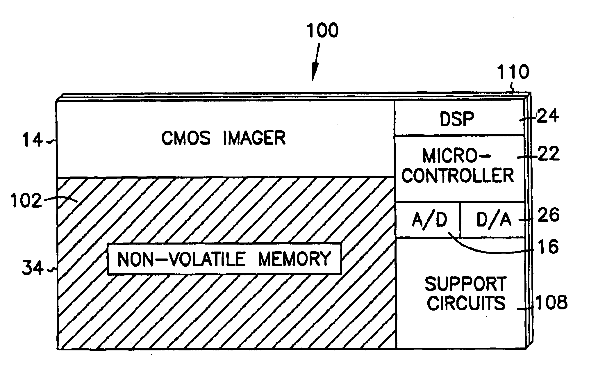
CMOS technology allows the fabrication of a single chip set having image capture, analog/digital conversion, digital processing and image storing capabilities. Image storing capabilities eliminates the need for placing non-volatile memory on a separate chi

Problems solved by technology

However, CCD technology is quite complex, suffers from low yields, and is expensive due to specialized processing involved to produce such devices.
Moreover, integrating analog/digital convertors and digital processing with a CCD array on the same chip is not feasible.
An imaging sensing device having a multiple chip set package is more costly to produce than a device utilizin

Method used


Image

  • CMOS imager with integrated non-volatile memory
  • CMOS imager with integrated non-volatile memory
  • CMOS imager with integrated non-volatile memory

Examples


Example

In the following detailed description of the preferred embodiments, reference is made to the accompanying drawings which form a part hereof, and in which is shown by way of illustration specific preferred embodiments in which the inventions may be practiced. These embodiments are described in sufficient detail to enable those skilled in the art to practice the invention, and it is to be understood that other embodiments may be utilized and that logical, mechanical and electrical changes may be made without departing from the scope of the present invention. The following detailed description is, therefore, not to be taken in a limiting sense, and the scope of the present inventions is defined only by the appended claims.

The terms wafer and substrate used in the following description include any structure having an exposed surface with which to form the integrated circuit (IC) structure of the invention. The term substrate is understood to include semiconductor wafers. The term substr...


PUM


Abstract

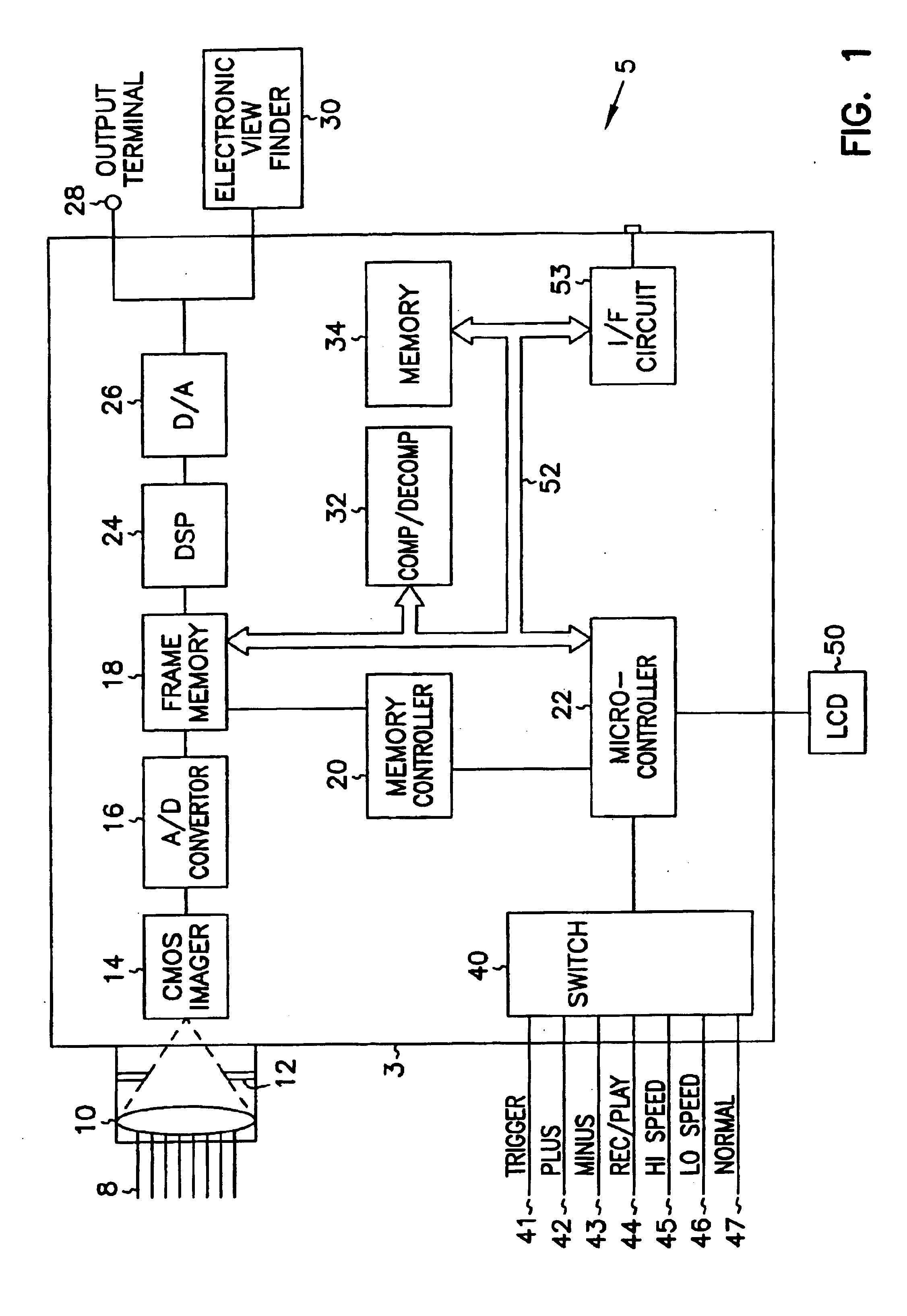
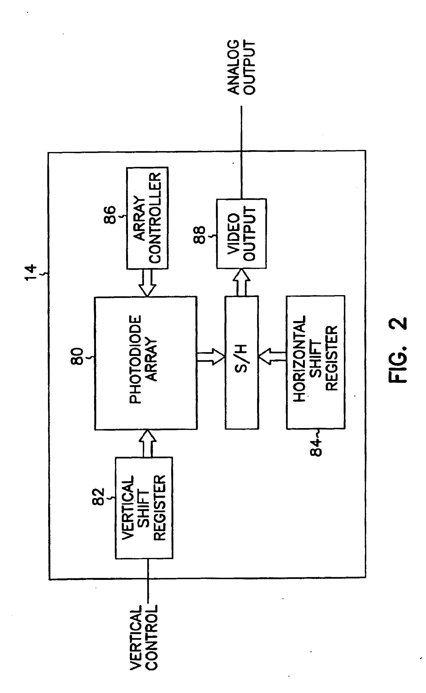
A CMOS imager and non-volatile memory are integrated on a single substrate along with logic and support circuitry for decoding and processing optical information received by the CMOS imager. A protective layer covers the non-volatile memory contained on the substrate for blocking light received by the CMOS imager. The protective layer can be a metal layer used as an interconnect over other areas of the substrate or an opaque layer provided during the fabrication process. Integrating a CMOS imager, non-volatile memory and peripheral circuitry for decoding and processing optical information received by the CMOS imager allows for a single chip image sensing device, such as a digital camera.

Description

TECHNICAL FIELD OF THE INVENTIONThe present invention relates generally to image sensing devices and in particular to a complementary metal oxide semiconductor (CMOS) imager with integrated non-volatile memory.BACKGROUND OF THE INVENTIONWith the advent of multimedia communications, there arises the need for low-cost solid state imagers to complement communication devices and computers. An image input sensor is central to any teleconferencing and multimedia application and is used to convert an optical image focused on the sensor into electrical signals. The image input sensor typically includes an array of light detecting elements where each element produces a signal corresponding to the intensity of light impinging on that element when an image is focused on the array. These signals may then be used, for example, to display a corresponding image on a monitor or to help record information about the optical image, as performed by a digital camera.A common type of image sensor is a ch...

Claims


Application Information

Patent Timeline
IPC IPC(8): H04N5/225H04N5/374H04N5/378H04N5/77H04N5/907H04N9/804
CPCH04N5/335H04N5/772Y10S438/945H04N9/8047H04N5/907H04N25/00
Inventor CHEVALLIER, CHRISTOPHE J.
Owner MICRON TECH INC
Why Eureka
Try Eureka