Multi-layer polishing pad material for CMP

a polishing pad and multi-layer technology, applied in the direction of flexible wheel, manufacturing tools, lapping machines, etc., can solve the problems of imperfect or degraded bonding of the pad layer or windows to the polishing pad, harsh fumes of adhesives,

Inactive Publication Date: 2005-04-26
CMC MATERIALS INC
View PDF16 Cites 84 Cited by
  • Summary
  • Abstract
  • Description
  • Claims
  • Application Information

AI Technical Summary

Benefits of technology

[0007]The invention provides a multi-layer polishing pad for use in chemical-mechanical polishing. The polishing pad comprises a polishing layer and a bottom layer, wherein the polishing layer and bottom layer are substantially coextensive and are joined together without the use of an adhesive. The invention also provides a polishing pad comprising a multi-layer optically transmissive region comprising two or more layers that are substantially coextensive and are joined together without the use of an adhesive.

Problems solved by technology

For example, the adhesives often have harsh fumes associated with them and typically require curing over 24 hours or more.
Moreover, the adhesive can be susceptible to chemical attack from the components of the polishing composition, and so the type of adhesive used in joining pad layers or attaching a window to the pad has to be selected on the basis of what type of polishing system will be used.
Furthermore, the bonding of the pad layers or windows to the polishing pad is sometimes imperfect or degrades over time.
This can result in delamination and buckling of the pad layers and / or leakage of the polishing composition between the pad and the window.
In some instances, the window can become dislodged from the polishing pad over time.
Methods for forming integrally molded polishing pad windows can be successful in avoiding at least some of these problems, but such methods are often costly and are limited in the type of pad materials that can be used and the type of pad construction that can be produced.

Method used


Image

  • Multi-layer polishing pad material for CMP
  • Multi-layer polishing pad material for CMP
  • Multi-layer polishing pad material for CMP

Examples


example

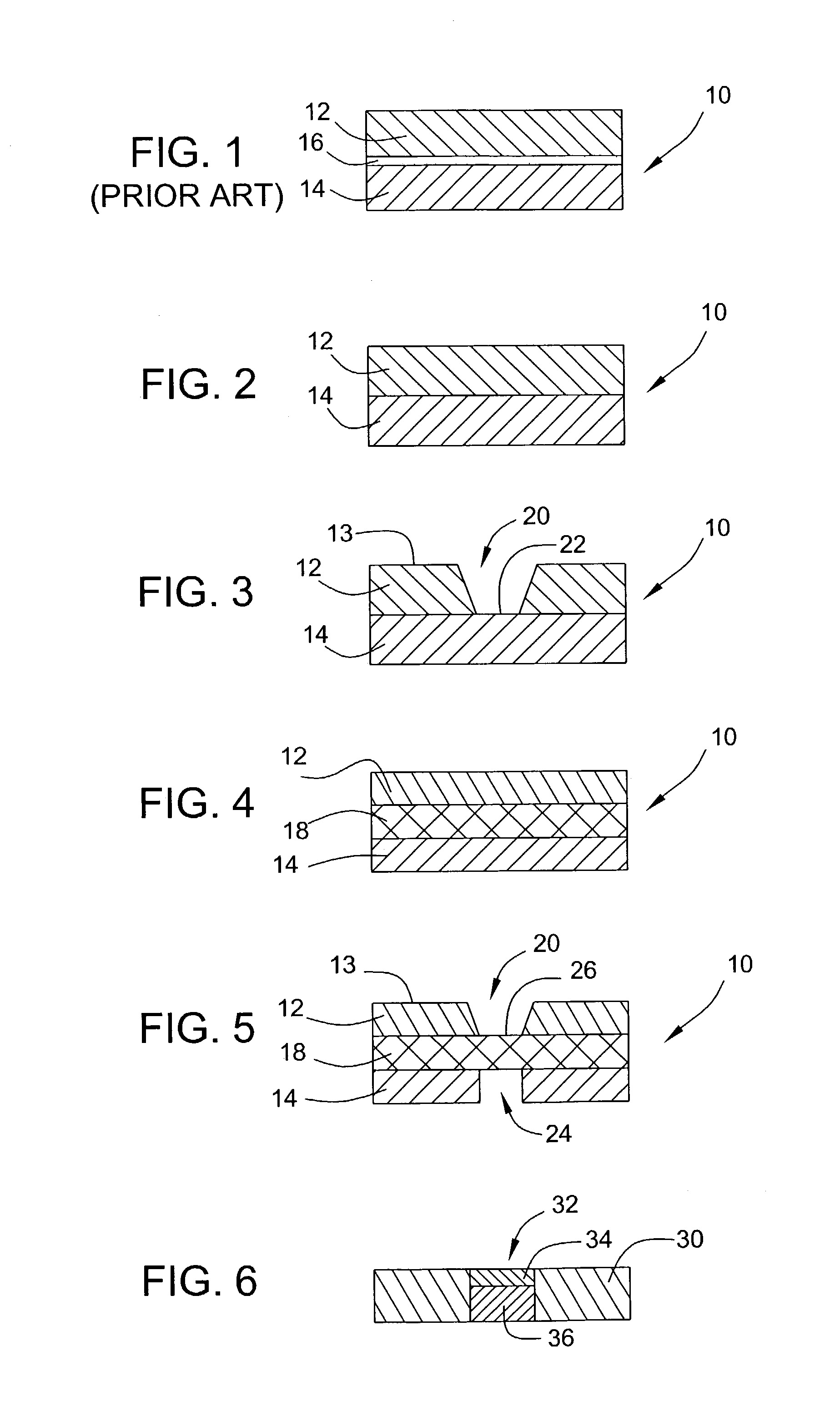
[0058]This example illustrates a method of producing a multi-layer polishing pad of the invention comprising a porous layer bound to a non-porous layer without the use of an adhesive.

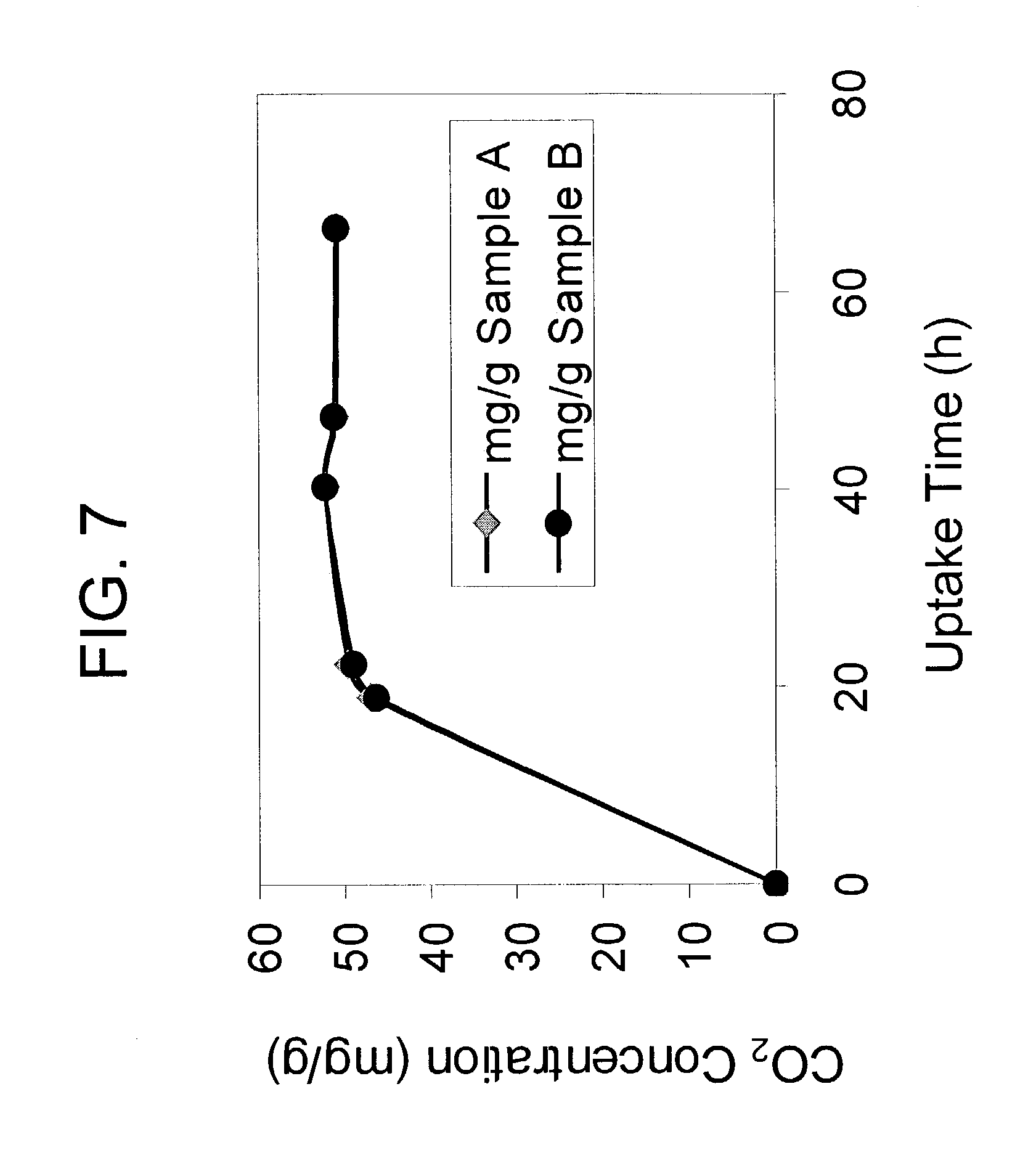
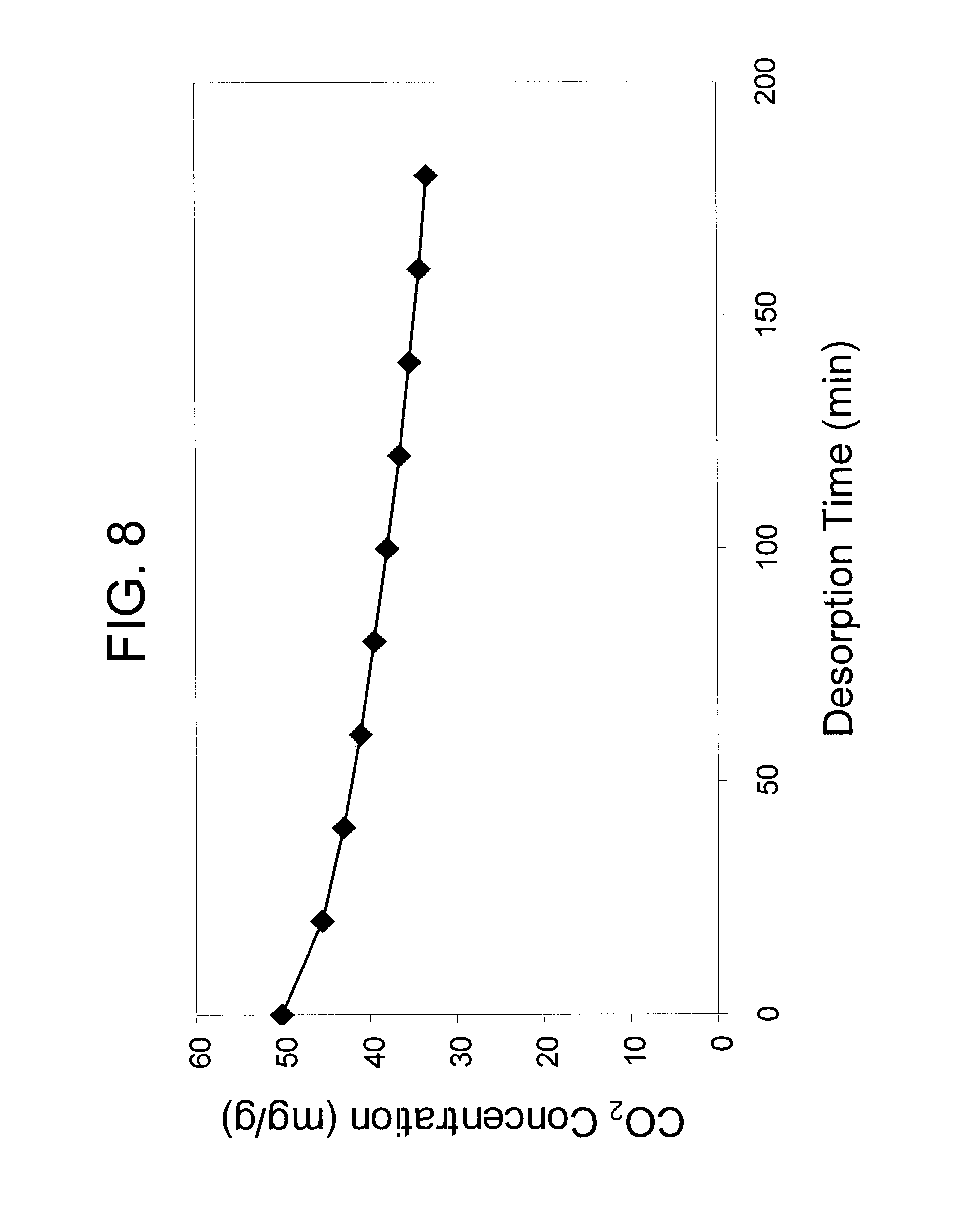
[0059]Solid thermoplastic polyurethane sheets (Samples A and B) having an average thickness of about 1500 μm were saturated with CO2 (approximately 50 mg / g thermoplastic polyurethane sample) at room temperature and 5 MPa pressure. A plot of the CO2 uptake as a function of time is shown in FIG. 7. The CO2-saturated samples A and B were then held at room temperature and atmospheric pressure for 20 minutes and 120 minutes, respectively, during which time partial desorption of the CO2 from the polymer sheet occurred. A plot of the CO2 loss as a function of time is shown in FIG. 8. The amount of CO2 loss form the samples was 4.5 mg / g (9%) and 13.5 mg / g (27%) thermoplastic polyurethane sample, respectively. After partial desorption, samples A and B were foamed at 93° C. SEM images of foamed samples A and B a...


PUM


Abstract

The invention is directed to a multi-layer polishing pad for chemical-mechanical polishing comprising a polishing layer and a bottom layer, wherein the polishing layer and bottom layer are joined together without the use of an adhesive. The invention is also directed to a polishing pad comprising an optically transmissive multi-layer polishing pad material, wherein the layers of the polishing pad material are joined together without the use of an adhesive.

Description

FIELD OF THE INVENTION[0001]This invention pertains to an adhesive-free multi-layer polishing pad material for use in chemical-mechanical polishing.BACKGROUND OF THE INVENTION[0002]Chemical-mechanical polishing (“CMP”) processes are used in the manufacturing of microelectronic devices to form flat surfaces on semiconductor wafers, field emission displays, and many other microelectronic substrates. For example, the manufacture of semiconductor devices generally involves the formation of various process layers, selective removal or patterning of portions of those layers, and deposition of yet additional process layers above the surface of a semiconducting substrate to form a semiconductor wafer. The process layers can include, by way of example, insulation layers, gate oxide layers, conductive layers, and layers of metal or glass, etc. It is generally desirable in certain steps of the wafer process that the uppermost surface of the process layers be planar, i.e., flat, for the deposit...

Claims


Application Information

Patent Timeline
Patent Type & Authority Patents(United States)
IPC IPC(8): B24D3/20B24D3/32B24B37/04B24D13/00B24D13/14B24B7/30B24B37/20
CPCB24D3/32B24B37/205B24D3/008B24D13/00
Inventor PRASAD, ABANESHWARSEVILLA, ROLAND K.LACY, MICHAEL S.
Owner CMC MATERIALS INC
Why Eureka
Try Eureka