Field effect transistor with stressed channel and method for making same

a field effect transistor and channel technology, applied in transistors, electrical devices, semiconductor devices, etc., can solve the problems of mechanical stress in microfabricated fets and cmos devices, inability to mass produce integrated circuits, and inability to achieve mass production integrated circuits. , to achieve the effect of stress in the channel

Inactive Publication Date: 2005-04-26
GLOBALFOUNDRIES INC
View PDF2 Cites 38 Cited by
  • Summary
  • Abstract
  • Description
  • Claims
  • Application Information

AI Technical Summary

Benefits of technology

[0012]The present invention includes a method for making a field effect transistor with longitudinal stress. The method includes forming an undercut area under the channel, and then forming a compressive film in the undercut area. The compressive film in the undercut area pushes up on the channel, thereby creating stress in the channel. The channel can be released in a middle portion. The undercut area can be formed by etching a buried oxide layer under the channel.
[0013]Also, the present invention includes a field effect transistor having a buried oxide layer, a channel disposed on the buried oxide layer, an undercut area under the channel, and a gate disposed over the channel. A compressive film is disposed in the undercut area, and the compressive film creates longitudinal stress in the channel. The undercut area may be formed by etching the buried oxide layer.

Problems solved by technology

However, incorporating mechanical stress into microfabricated FETs and CMOS devices has proven difficult.
However, this technique is not practical for mass producing integrated circuits.
One significant problem with employing stress is that PFET and NFET devices require opposite stress.
The compressive film in the undercut area pushes up on the channel, thereby creating stress in the channel.

Method used


Image

  • Field effect transistor with stressed channel and method for making same
  • Field effect transistor with stressed channel and method for making same
  • Field effect transistor with stressed channel and method for making same

Examples


Embodiment Construction

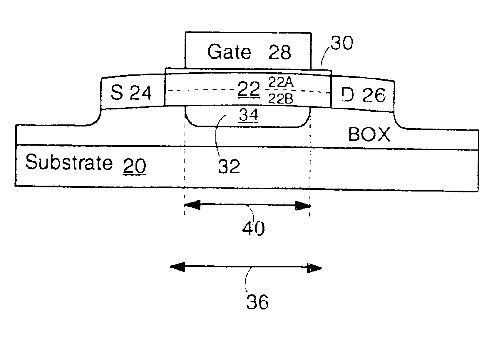
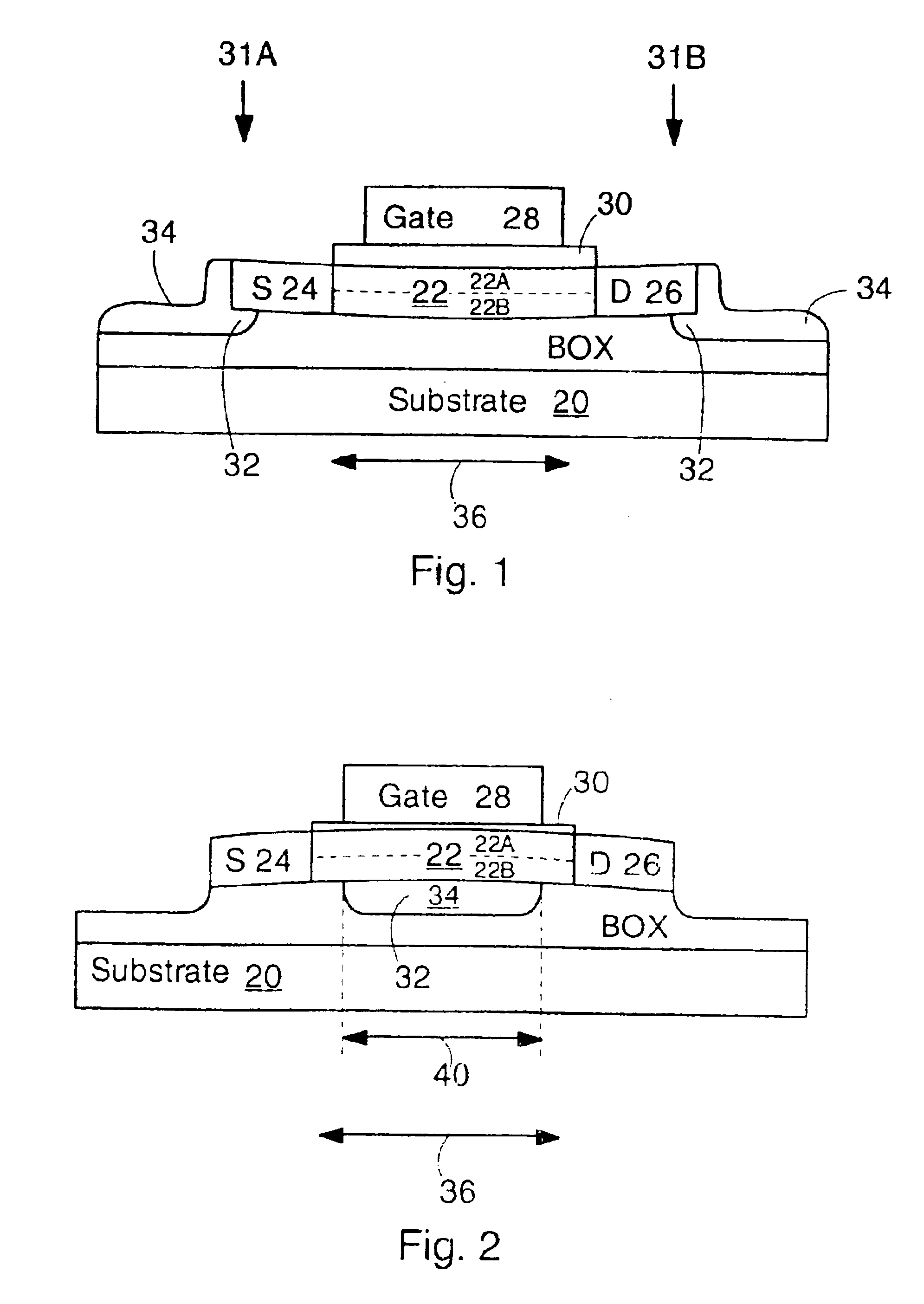
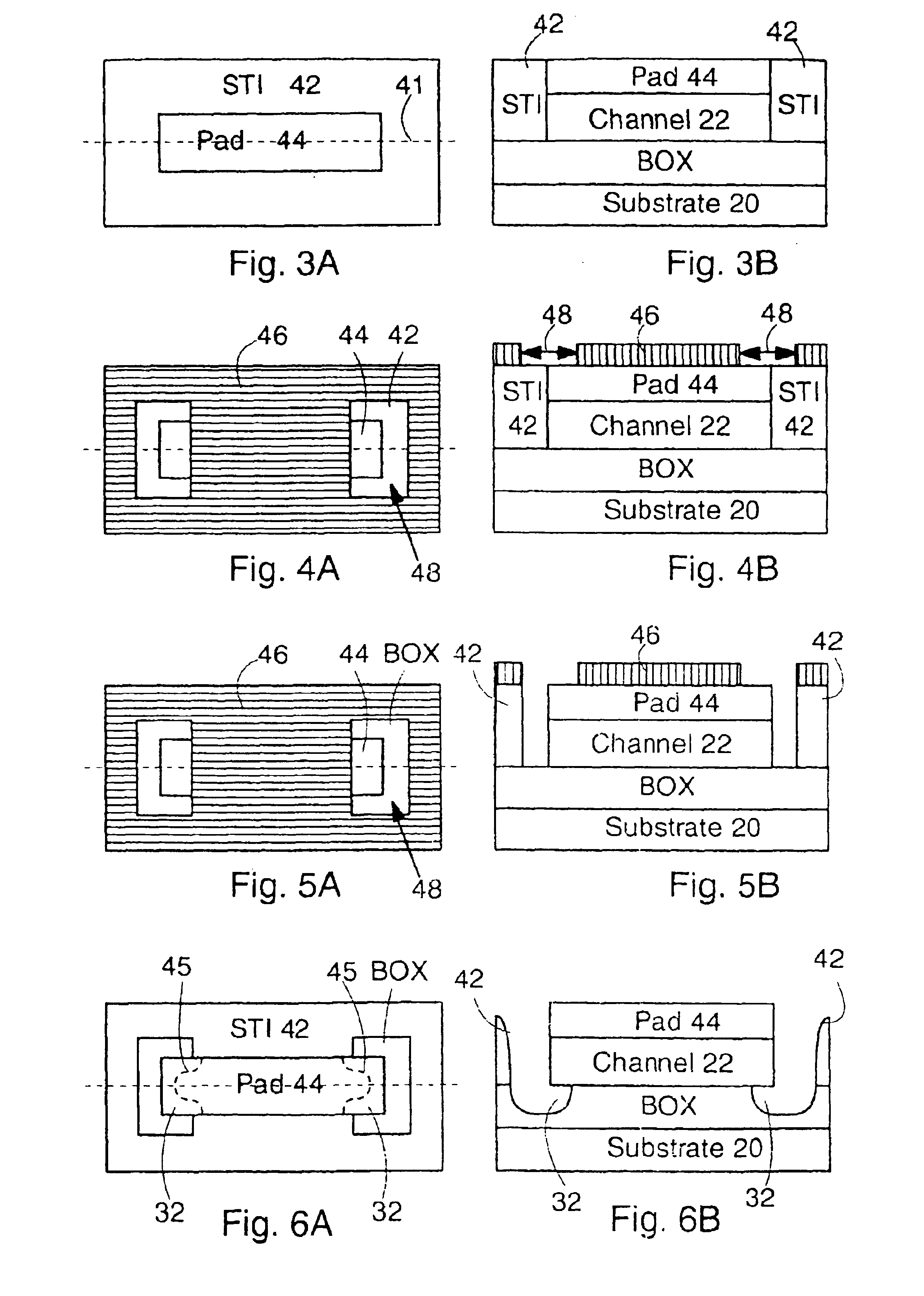
[0018]The present invention provides both NFET and PFET field effect transistors (e.g. CMOS devices) having stressed channel regions for enhanced charge carrier mobility. The present invention also provides a method for fabricating FETs with stressed channels. In the present invention, edges of the channel region are undercut (e.g. by an isotropic etchant). Then, a compressive film is deposited in the undercut areas. The compressive film pushes upwards on the channel from the undercut areas, thereby bending the channel, and inducing stress in the channel. Depending on the placement of the compressive thin film, the longitudinal stress in the channel will be compressive or tensile. The type of stress (i.e. compressive or tensile) is selected to produce desired performance alterations in the FET. Specifically, PFET devices require longitudinal compressive stress for charge mobility increase, and NFET devices require longitudinal tensile stress for charge mobility increase.

[0019]FIG. 1...


PUM


Abstract

Field effect transistor with increased charge carrier mobility due to stress in the current channel 22. The stress is in the direction of current flow (longitudinal). In PFET device, the stress is compressive; in NFET devices, the stress is tensile. The stress is created by a compressive film 34 in an area 32 under the channel. The compressive film pushes up on the channel 22, causing it to bend. In PFET devices, the compressive film is disposed under ends 31 of the channel (e.g. under the source and drain), thereby causing compression in an upper portion 22A of the channel. In NFET devices, the compressive film is disposed under a middle portion 40 of the channel (e.g. under the gate), thereby causing tension in the, upper portion of the channel. Therefore, both NFET and PFET device can be enhanced. A method for making the devices is included.

Description

[0001]This application is a division of U.S. patent application Ser. No. 10 / 318,601, filed Dec. 12, 2002, now U.S. Pat. No. 6,717,216.BACKGROUND OF THE INVENTION[0002]1. Field of the Invention[0003]The present invention relates generally to field effect transistors such as CMOS transistors. More particularly, the present invention relates to a method for forming field effect transistors with stressed channel regions which provide increased drive current capability among other benefits.[0004]2. Background Description[0005]Field effect transistors such as CMOS transistors are widely used in the electronics industry. Field effect transistors (FETs) are employed in almost every electronic circuit application, such as signal processing, computing, and wireless communications. There is constantly a demand for improved field effect transistor performance. Performance metrics that may be of interest include switching speed, on-state current capability, and on-state to off-state current rati...

Claims


Application Information

Patent Timeline
Patent Type & Authority Patents(United States)
IPC IPC(8): H01L21/02H01L21/70H01L29/66H01L27/12H01L21/336H01L29/786H01L21/84H01L27/08H01L21/8238H01L27/092H01L29/78
CPCH01L21/84H01L27/1203H01L29/78696H01L29/7842H01L29/78603H01L29/66772H01L29/78
Inventor DORIS, BRUCE B.CHIDAMBARRAO, DURESETIBAIE, XAVIERMANDELMAN, JACK A.SADANA, DEVENDRA K.SCHEPIS, DOMINIC J.
Owner GLOBALFOUNDRIES INC
Why Eureka
Try Eureka