Multiple user interfaces for an integrated flash device

a flash device and interface technology, applied in the field of integrated circuit interfaces, can solve the problems of adding to the total pin count of the packaged device, and being undesirable to disclose a proprietary interface to the publi

Inactive Publication Date: 2005-04-26
INTEL CORP
View PDF11 Cites 12 Cited by
  • Summary
  • Abstract
  • Description
  • Claims
  • Application Information

AI Technical Summary

Problems solved by technology

One problem with such a device is that the use of dedicated pins adds to the total pin count of the packaged device, thereby necessitating the use of a larger package.
One problem with providing a device interface specification is that it may be undesirable to disclose a proprietary interface to the public.

Method used


Image

  • Multiple user interfaces for an integrated flash device
  • Multiple user interfaces for an integrated flash device
  • Multiple user interfaces for an integrated flash device

Examples


Embodiment Construction

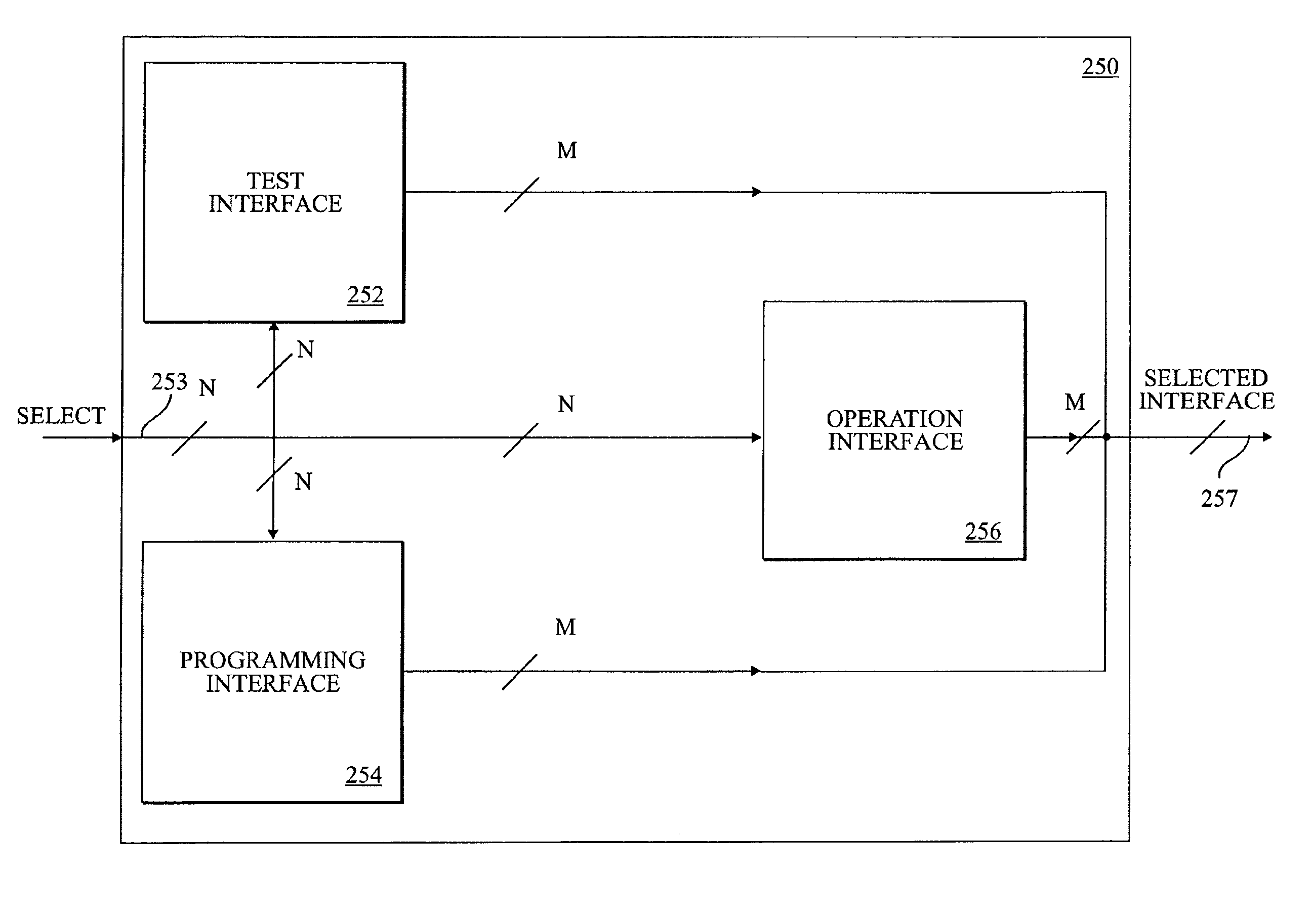
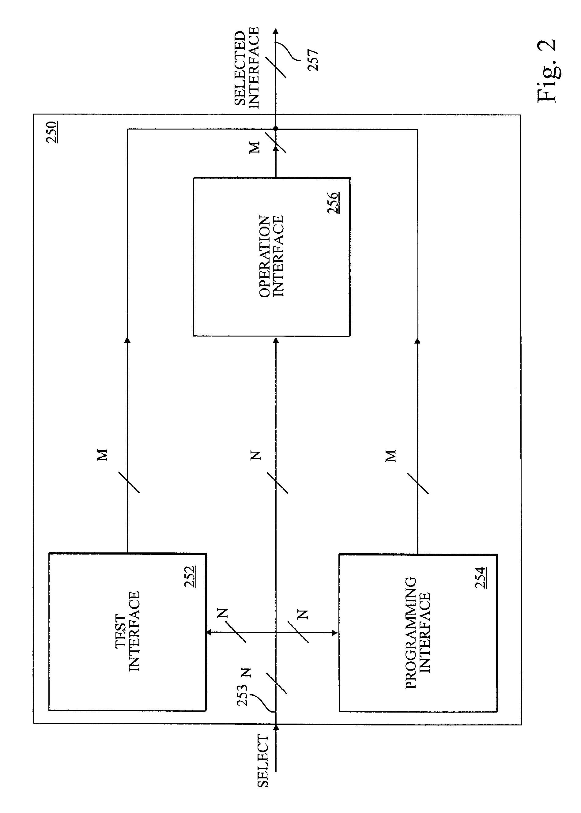
[0017]A memory device having multiple interfaces is described. The memory device may be configured to operate with different interfaces by using selection circuitry to switch device circuitry connected to device pads. For one of the embodiments, the memory device includes a test interface to test the memory device for defects, a programming interface to program the memory device with a code, and an operation interface to operate the memory device in a computer system. The use of multiple interfaces may reduce the pin count of the packaged memory device by providing for the use of existing device pads to program the memory device. A reduced pin count may also allow for integration of non-memory logic functions, for example, general purpose input pins.

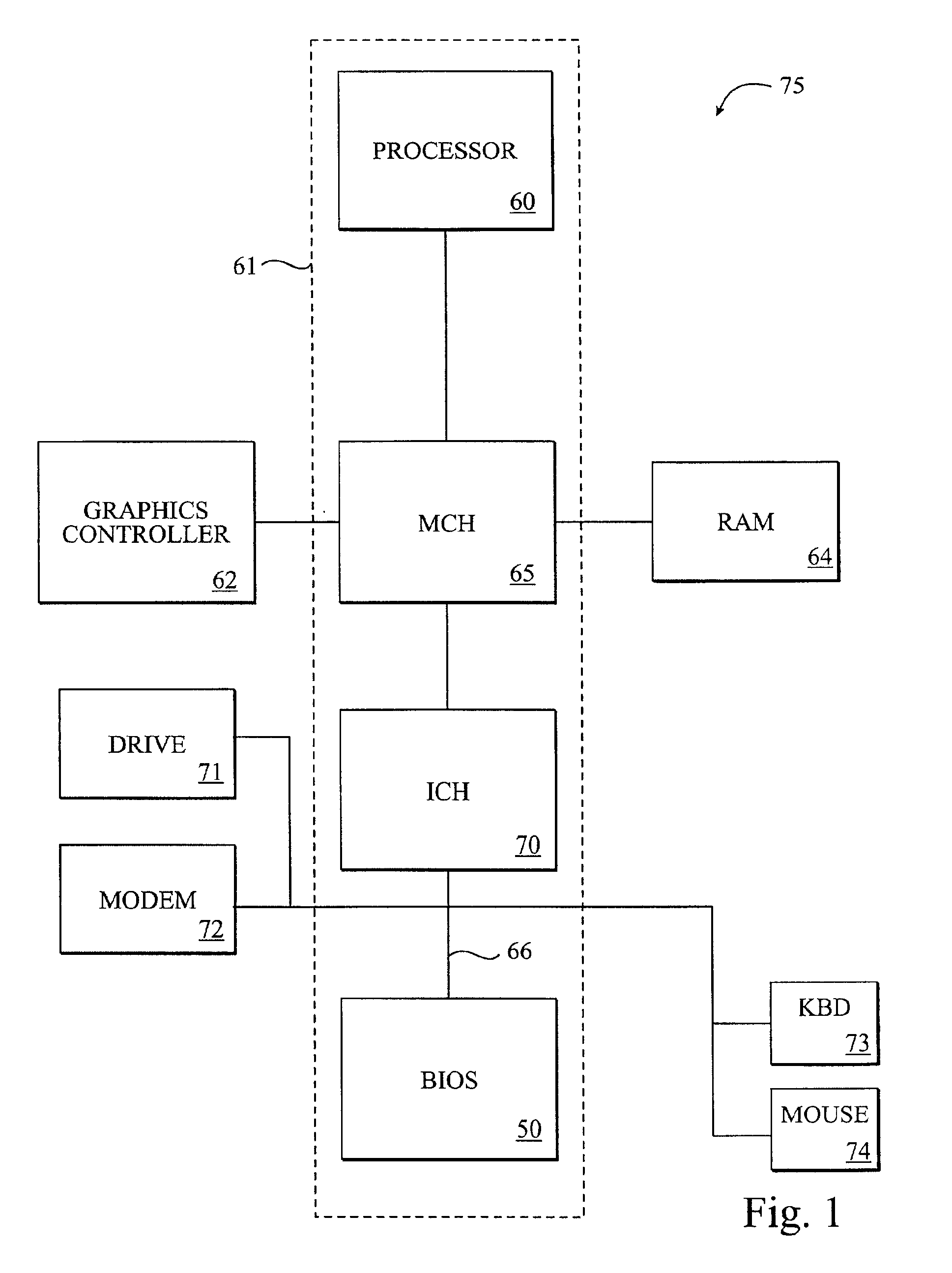
[0018]FIG. 1 illustrates one embodiment of a computer system containing a memory component having multiple interfaces. Computer system 75 includes a processor 60, a memory control hub (MCH) 65, an input / output control hub (ICH) 70, and a...


PUM


Abstract

A memory device having multiple interfaces is described. The memory device may be configured to operate with different interfaces using configuration circuitry in the device that enables switching between the multiple interfaces.

Description

[0001]This is a continuation of application Ser. No. 09 / 293,576, filed Apr. 16, 1999 now U.S. Pat. No. 6,330,635.FIELD OF THE INVENTION[0002]This invention relates to the field of integrated circuits and, more specifically, to interfaces for integrated circuits.BACKGROUND[0003]The motherboard is the main circuit board inside a computer which holds the processor, memory, and expansion slots and connects directly or indirectly to every part of the computer. The motherboard contains a control chipset, a memory device storing code, and the various buses used to link the motherboard components.[0004]Typically, the memory on a motherboard is a Basic Input Output System (BIOS) memory component. BIOS consists of low-level code in a memory component that enables communication between the computer's operating system and hardware, including peripheral technologies. The BIOS also provides the initial instructions for power on self-test and booting system files. The BIOS component is tested by t...

Claims


Application Information

Patent Timeline
Patent Type & Authority Patents(United States)
IPC IPC(8): G06F13/40
CPCG06F13/4004
Inventor STAFFORD, WILLIAM R.
Owner INTEL CORP
Why Eureka
Try Eureka