Latch circuit for latching a pair of complementary data signals

a latch circuit and complementary data technology, applied in the direction of pulse manipulation, pulse technique, instruments, etc., can solve the problems of large increased time length needed for the discharge and injection of electric charges, and malfunction of the latch circuit in the signal transmission. , to achieve the effect of reducing the dead zone of the latch circuit, reducing the time length of the signal inversion, and reducing the energy burden on the power source lin

Inactive Publication Date: 2005-05-03
RENESAS ELECTRONICS CORP
View PDF6 Cites 6 Cited by
  • Summary
  • Abstract
  • Description
  • Claims
  • Application Information

AI Technical Summary

Benefits of technology

[0013]In view of the above problem of the conventional latch circuit, it is an object of the present invention to provide a new latch circuit which is capable of reducing the time length for the signal inversion of the output complementary data signals by reducing the energy burden on the power source lines and thus reducing the dead zone of the latch circuit.
[0015]In accordance with the latch circuit of the present invention, the precharge section precharging the latch output nodes allows the signal inversion on the latch output nodes to be effected only by discharging electric charge from one of the latch output nodes during the hold period, thereby reducing the energy burden on the power source lines. This allows a higher-speed signal inversion of the complementary data signals, to thereby reduce the dead zone of the latch circuit including a setup time and a hold time thereof compared to the conventional latch circuit wherein both the discharge and injection occur concurrently during the sample period.
[0016]It is to be noted that the dead zone of the latch circuit is determined by the time length needed for updating the previous data stored in the latch circuit by a new data. If the time length needed for the signal inversion is short, the dead zone is small, whereas if this time length is long, the dead zone is large. In the latch circuit of the present invention, since the previous data stored in the latch circuit is first discarded by the precharge section during the sample period to allow the latch circuit to assume a neutral state, the energy needed for update of the data is thereby reduced to reduce the time length for the update of data. Thus, the dead zone of the latch circuit can be reduced.

Problems solved by technology

This causes a large energy burden on the power source lines VCC and GND, whereby the time length needed for the discharge and injection of the electric charge increases.
This may cause a malfunction of the latch circuit in the signal transmission depending on the delivery timing of the input complementary data signals.

Method used


Image

  • Latch circuit for latching a pair of complementary data signals
  • Latch circuit for latching a pair of complementary data signals
  • Latch circuit for latching a pair of complementary data signals

Examples


Embodiment Construction

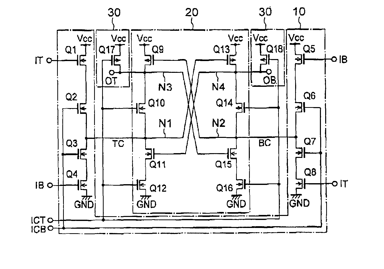
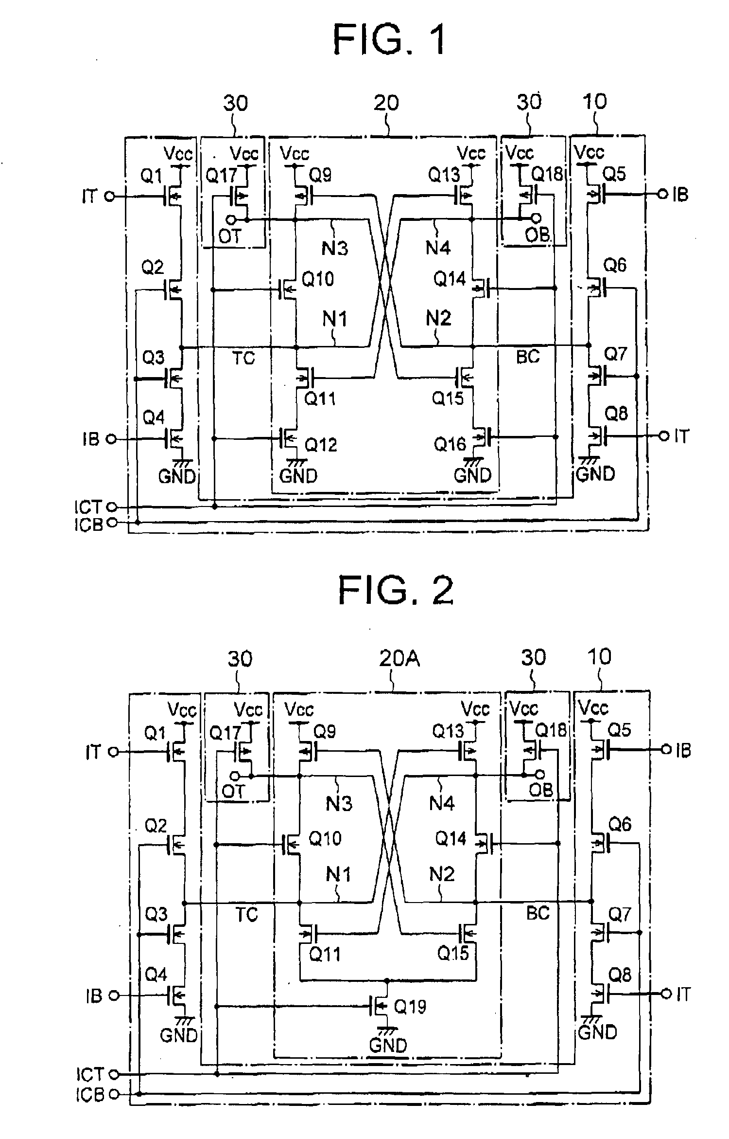
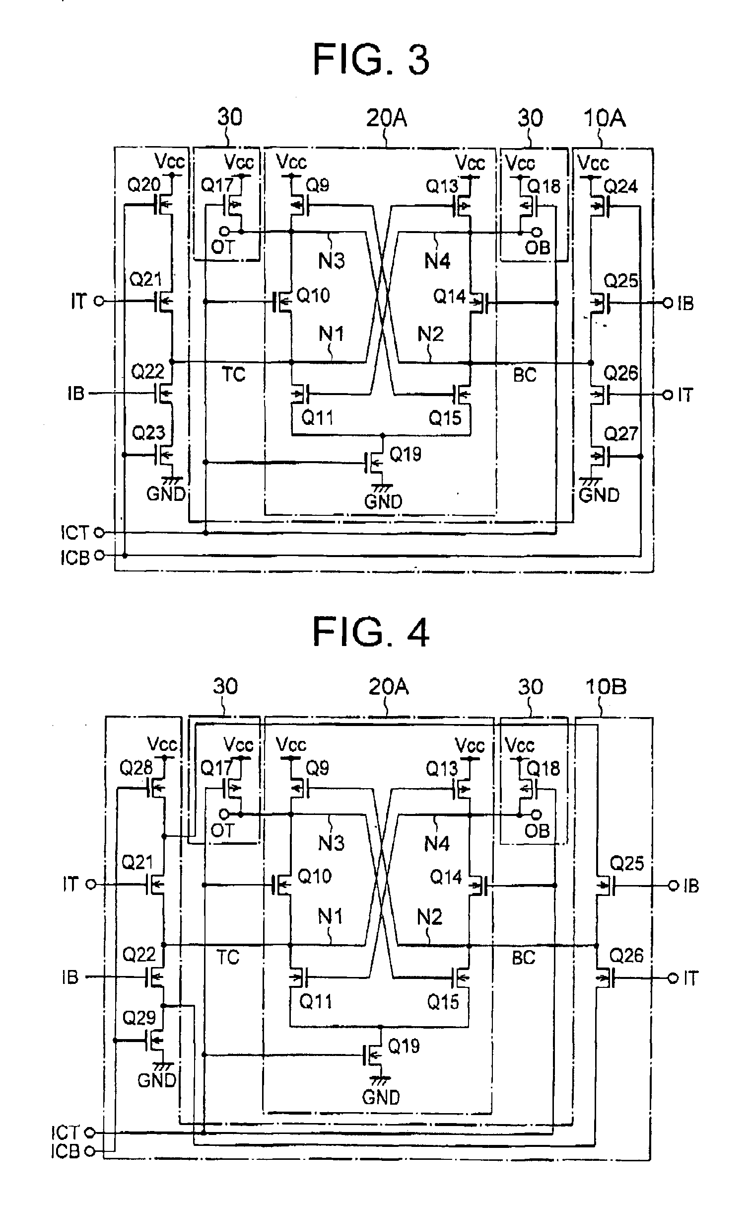
[0025]Now, the present invention is more specifically described with reference to accompanying drawings, wherein similar constituent elements are designated by similar reference numerals.

[0026]Referring to FIG. 1, a latch circuit according to a first embodiment of the present invention includes a sample section 10 for responding to a pair of complementary clock signals ICT and ICB to sample a pair of input complementary data signals IT and IB, a latch section 20 for latching the complementary data signals sampled by the sample section 10 to transmit the same to a next stage circuit (not shown), and a precharge section 30 for precharging the output nodes N3 and N4 of the latch section (referred to as latch output nodes N3 and N4) during a sample period.

[0027]The sample section 10 includes a first data input block including four n-channel transistors (nMOSFETs) Q1 to Q4 connected in series from the high-potential power source line VCC to the low-potential power source line GND consecu...


PUM


Abstract

A latch circuit includes a sample section for responding to complementary clock signals to sample complementary data signals during a sample period, a latch section for latching the sampled complementary data signals on latch output nodes to transfer the same through latch output nodes during a hold period, and a precharge section for precharging the latch output nodes during the sample period. The latch circuit has a smaller dead zone including a smaller setup time and a smaller hold time.

Description

BACKGROUND OF THE INVENTION[0001](a) Field of the Invention[0002]The present invention relates to a latch circuit for latching a pair of complementary data signals and, more particularly, to a latch circuit which responds to a pair of complementary clock signals to latch a pair of complementary data signals.[0003](b) Description of the Related Art[0004]A latch circuit is known which responds to a pair of complementary clock signals to latch and transfer a pair of input complementary data signals. A CMOS circuit is generally used for such a latch circuit. FIG. 6 shows a conventional latch circuit, which is described in Patent Publication JP-A-2001-21786.[0005]The latch circuit of FIG. 6 includes a sample section 10C activated by one of a complementary clock signals ICT and ICB to sample a pair of input complementary data signals IT and IB, and a latch section 20C activated by the other of the complementary clock signals ICT and ICB to latch the complementary data signals sampled by t...

Claims


Application Information

Patent Timeline
Patent Type & Authority Patents(United States)
IPC IPC(8): G11C27/02G11C27/00H03K3/356
CPCG11C27/02
Inventor AOKI, YASUSHI
Owner RENESAS ELECTRONICS CORP
Why Eureka
Try Eureka