

Transmission line with a projecting dielectric part having an opposing coplanar line and transceiver
a dielectric part and transceiver technology, applied in the field of transmission lines, can solve the problems of large losses at connection points, and achieve the effect of reducing conductor losses and being easy to connect to a semiconductor elemen
- Summary
- Abstract
- Description
- Claims
- Application Information
AI Technical Summary
Benefits of technology
Problems solved by technology
Method used
Image

Examples
first embodiment
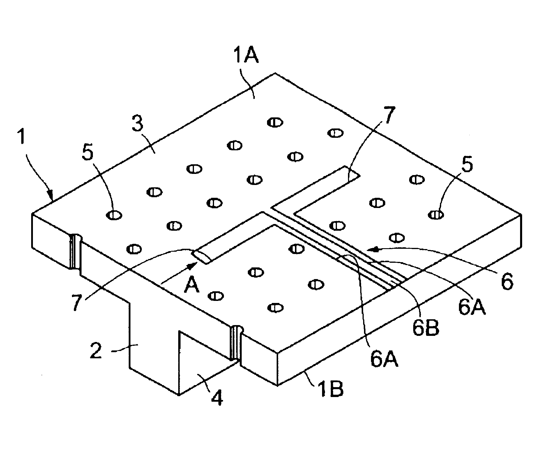
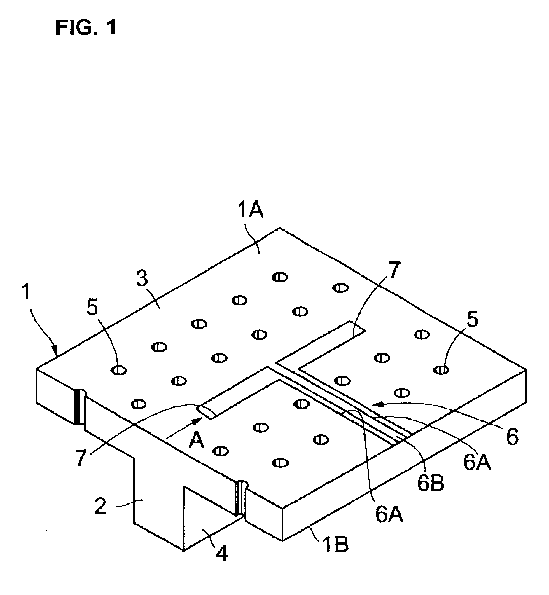
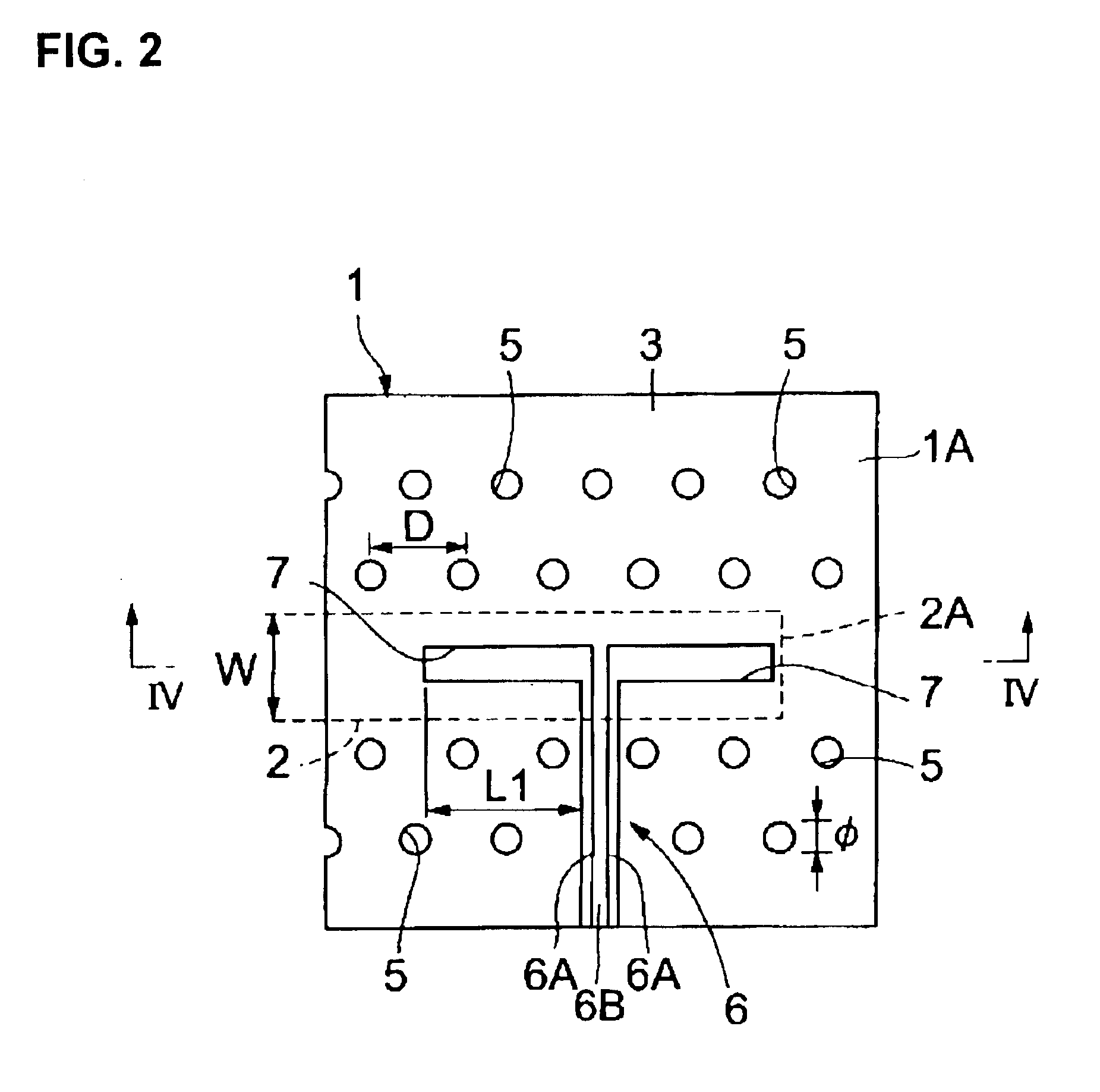
[0041]FIGS. 1 to 5 illustrate the transmission line according to the present invention. The transmission line includes a dielectric substrate 1 comprising a resin material, a ceramic material, or the like. The dielectric substrate 1 preferably has a flat shape and has a relative dielectric constant (εr) of about 7.0 and a thickness H1 (FIG. 4) of about 0.3 mm. On a top surface 1A (FIGS. 1-4) of the dielectric substrate 1, a coplanar line 6 (FIGS. 1, 2, 3, and 5) is formed. On a bottom surface 1B (FIGS. 1, 3, 4) of the dielectric substrate1, a projecting part 2 (FIGS. 1-4) is formed. The projecting part 2 has protruding cross section and extends along a direction along which RF signals, such as microwave signals and EHF signals, are transmitted (a direction represented by arrow A).
[0042]The lateral width W (FIG. 2) of the projecting part 2 is, for example, about 0.45 mm. The lateral width W is set, for example, so as to be smaller than λg / 2 in relation to the wavelength λg of an RF s...
second embodiment
[0060]Therefore, in the case where the transmission line is used, by setting the length L2 of each slot 11, the length L3 of each short-circuited stub 12, and so forth as required, it becomes possible to adjust the impedance of an entire circuit of the slots 11, including two coils and the two short-circuited stubs. Further, by setting the length L3 of each short-circuited stub 12 as required, it becomes possible to adjust the impedance of an overall circuit including the short-circuited stubs 12 and the coplanar line 6. Subsequently, the difference between the impedance of the circuit of the slots-11-side and the impedance of the circuit of the coplaner-line-6-side is reduced. Therefore, the reflection loss between the two circuits is reduced and a transmission characteristic shown in FIG. 10 is obtained.
[0061]As a result, when the frequency of the RF signal is about 75 GHz, the reflection coefficient S11 between the waveguide in the dielectric substrate 1 and the coplanar line 6 ...
third embodiment
[0068]Accordingly, in a case where the transmission line of the third embodiment is used, the impedance of an entire circuit of the slots 21, including two coils and the two short-circuited stubs, can be adjusted by changing the length L5 of the short-circuited stubs 22, the length L4 of the slots 21, the angle θ, and so forth. Further, the impedance of an entire circuit including the short-circuited stubs 22 and the coplanar line 6 can be adjusted by changing the length L5 of the short-circuited stubs 22 as required. Subsequently, the difference between the impedance of the circuit on the slots-21-side and the impedance of the circuit on the coplanar-line-6-side can be further reduced. Further, reflection losses due to wide-band RF signals can be reduced. Therefore, a transmission characteristic such as that shown in FIG. 15 can be achieved.
[0069]As a result, when the frequency of the RF signal is about 72 to 82 GHz, the reflection coefficient S11 between the waveguide in the diele...
PUM
 Abstract
Description
Claims
Application Information