Check patentability & draft patents in minutes with Patsnap Eureka AI!

Multiple chip system including a plurality of non-volatile semiconductor memory devices

Inactive Publication Date: 2005-05-03
SAMSUNG ELECTRONICS CO LTD
View PDF4 Cites 20 Cited by
  • Summary
  • Abstract
  • Description
  • Claims
  • Application Information

AI Technical Summary

Benefits of technology

[0011]The first and second chips are adapted to o

Problems solved by technology

The tloss period deteriorates system performance.

Method used


Image

  • Multiple chip system including a plurality of non-volatile semiconductor memory devices
  • Multiple chip system including a plurality of non-volatile semiconductor memory devices
  • Multiple chip system including a plurality of non-volatile semiconductor memory devices

Examples


Embodiment Construction

[0018]The present invention will now be described more fully hereinafter with reference to the accompanying drawings, in which exemplary embodiments of the invention are shown. This invention may, however, be embodied in different forms and should not be constructed as limited to the embodiments set forth herein. Rather, these embodiments are provided so that this disclosure will be thorough and complete, and will fully convey the scope of the invention to those skilled in the art.

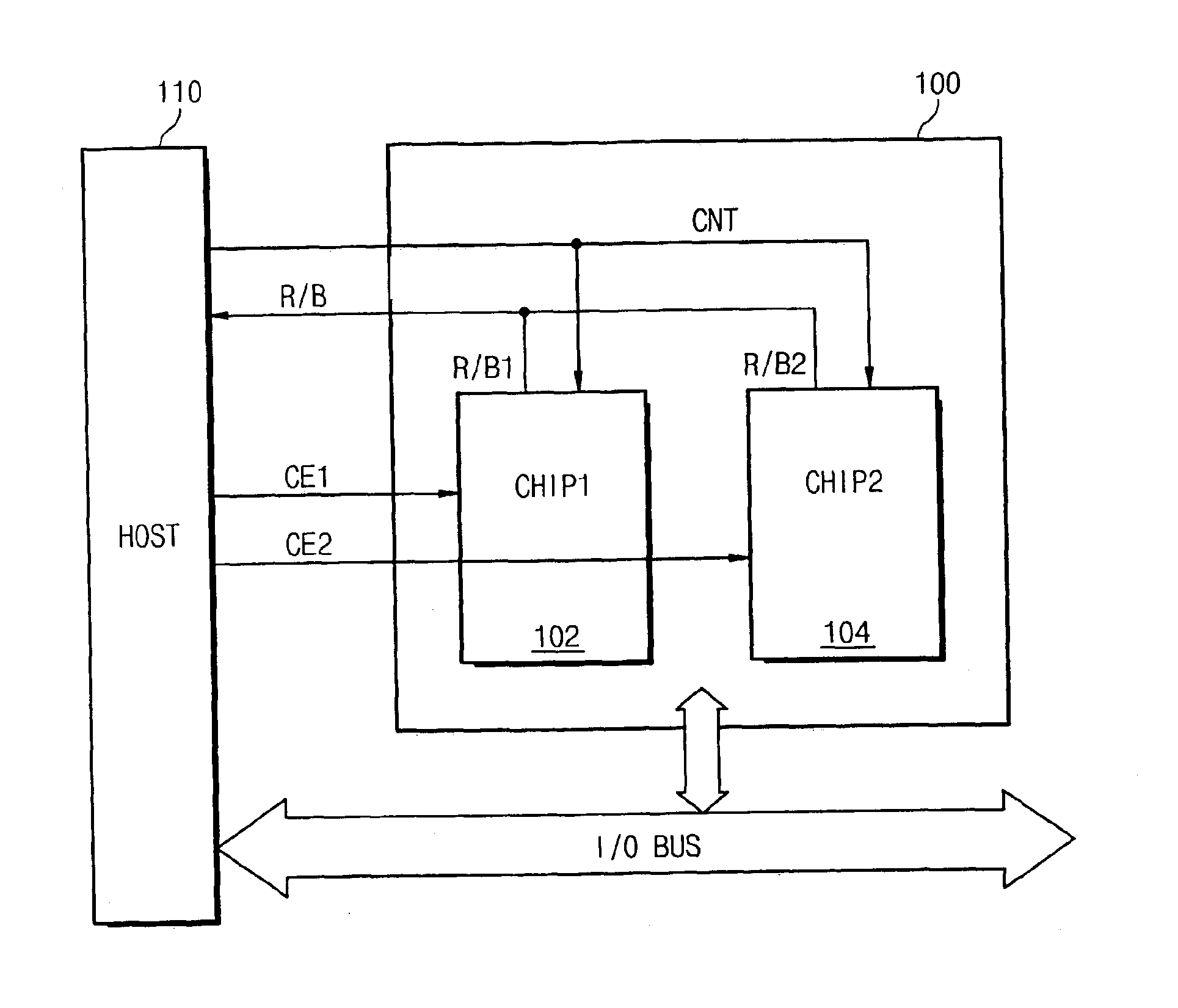
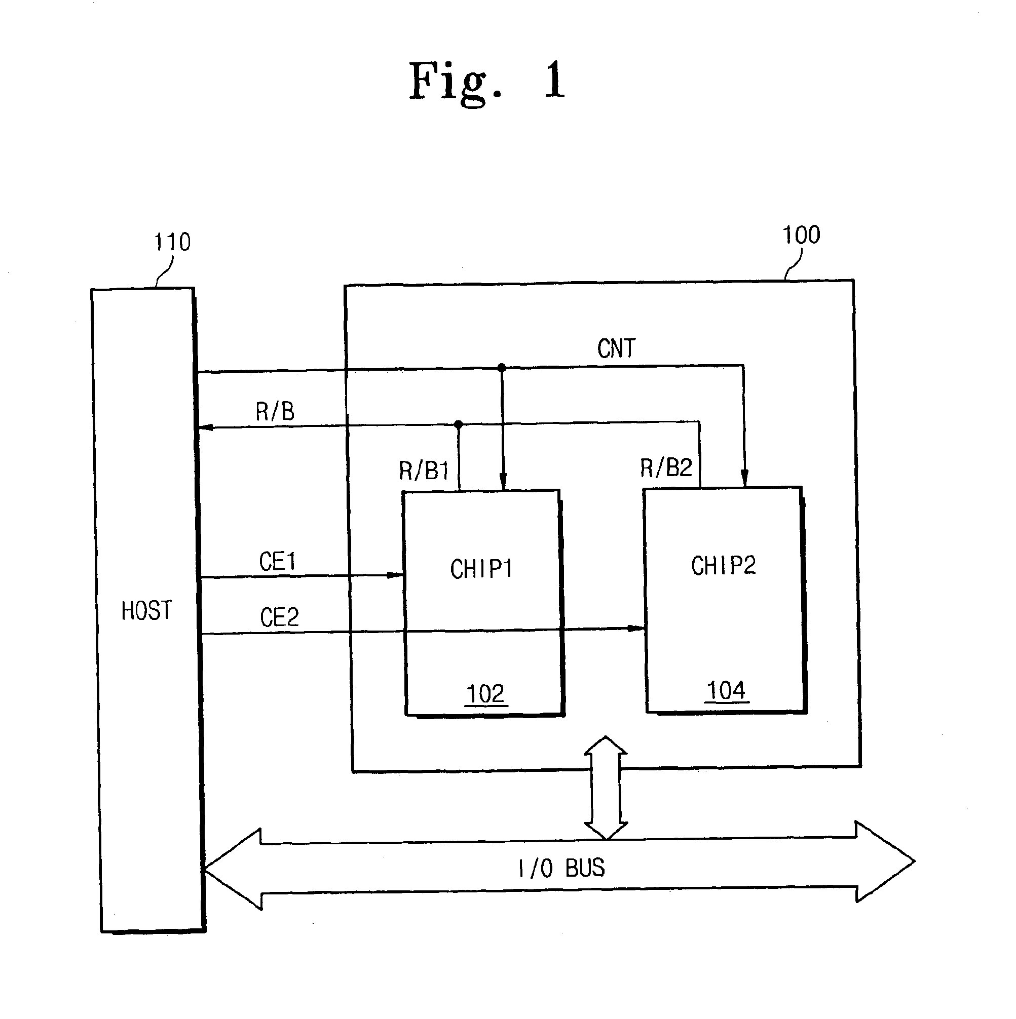
[0019]FIG. 3 is a block diagram of embodiment of a multiple chip memory system of the present invention. The multiple chip 300 includes first and second chips 302 and 304, respectively. The chip 30 interfaces to a host 310 by control signals CNT, a first chip selection signal CE1, a second chip selection signal CE2, a R / B 1 signal, and a R / B 2 signal. Input / output data DIO is interchanged between an input / output bus I / O BUS and the multiple chip 310. The host 310 includes a microprocessor (not shown) to co...


PUM


Abstract

A multiple chip memory system capable of providing state information relating to each chip embedded therein. The multiple chip memory system includes a first chip enabled by a first chip selection signal, and informing of a self state by a first ready / busy signal; and a second chip enabled by a second chip selection signal, and informing of a self state by a second ready / busy signal.

Description

FIELD OF THE INVENTION[0001]The present invention generally relates to a semiconductor memory device and, more specifically, to a multiple chip system embedding a plurality of non-volatile memory devices therein.BACKGROUND OF THE INVENTION[0002]The demand for electrically erasable and programmable non-volatile memory devices continues to increase in their applications. High capacity non-volatile memory devices are particularly advantageous because of successive developments with Riger frequencies and improved integration density.[0003]Several technologies exist to embed a plurality of non-volatile memory devices on one chip. Doping so enhances data storage capacity for digital multimedia such as an SSD (Solid State Disk) and expansion memory cards.[0004]FIG. 1 illustrates a conventional multiple chip memory system including a conventional multiple chip. Referring to FIG. 1, a first chip 102 and a second chip 104 are included in a multiple chip 100. A host 110 and the multi-chip 100 ...

Claims


Application Information

Patent Timeline
IPC IPC(8): G11C16/20G11C16/06G11C16/00G06F12/06
CPCG11C16/20G11C2029/4402G11C7/1063G11C16/00
Inventor JANG, CHEOL-UNGCHOI, YOUNG-JOON
Owner SAMSUNG ELECTRONICS CO LTD
Features
  • R&D
  • Intellectual Property
  • Life Sciences
  • Materials
  • Tech Scout
  • Unparalleled Data Quality
  • Higher Quality Content
  • 60% Fewer Hallucinations
Learn More