Apparatus and method for detecting photon emissions from transistors

a transistor and photon emission technology, applied in the direction of electronic circuit testing, measurement devices, instruments, etc., can solve the problems of difficult or impossible to physically test such small discrete elements of an ic, poor quantum efficiency of the available pmt detectors in the near infrared spectrum, and difficult to perform physical probing of the ic. easy to achieve the effect of reducing the time required, rapidly detecting the difference between photons emitted, and rapid extraction of transistor timing information

Inactive Publication Date: 2005-05-10
DCG SYST
View PDF57 Cites 21 Cited by
  • Summary
  • Abstract
  • Description
  • Claims
  • Application Information

AI Technical Summary

Benefits of technology

[0011]Aspects of the present invention dramatically reduce the time required to acquire a sufficient number of transistor emitted photons to extract useful information. Implementations of the present invention can be used to rapidly discriminate between photons emitted from transistors and background photon emissions. Implementations of the present invention may also be used to rapidly extract transistor timing information. In some instances, data acquisition times can be reduced from several hours or days, to only several minutes. With suc...

Problems solved by technology

Testing such small discrete elements of an IC is difficult or impossible to perform by physically probing the IC.
Moreover, physically probing the IC can easily damage it.
The quantum efficiency of the available PMT detectors is poor in the near infrared spectrum, but is higher in the visible spectrum.
The detection of 10 million or more photons may take hours or days,...

Method used


Image

  • Apparatus and method for detecting photon emissions from transistors
  • Apparatus and method for detecting photon emissions from transistors
  • Apparatus and method for detecting photon emissions from transistors

Examples


Embodiment Construction

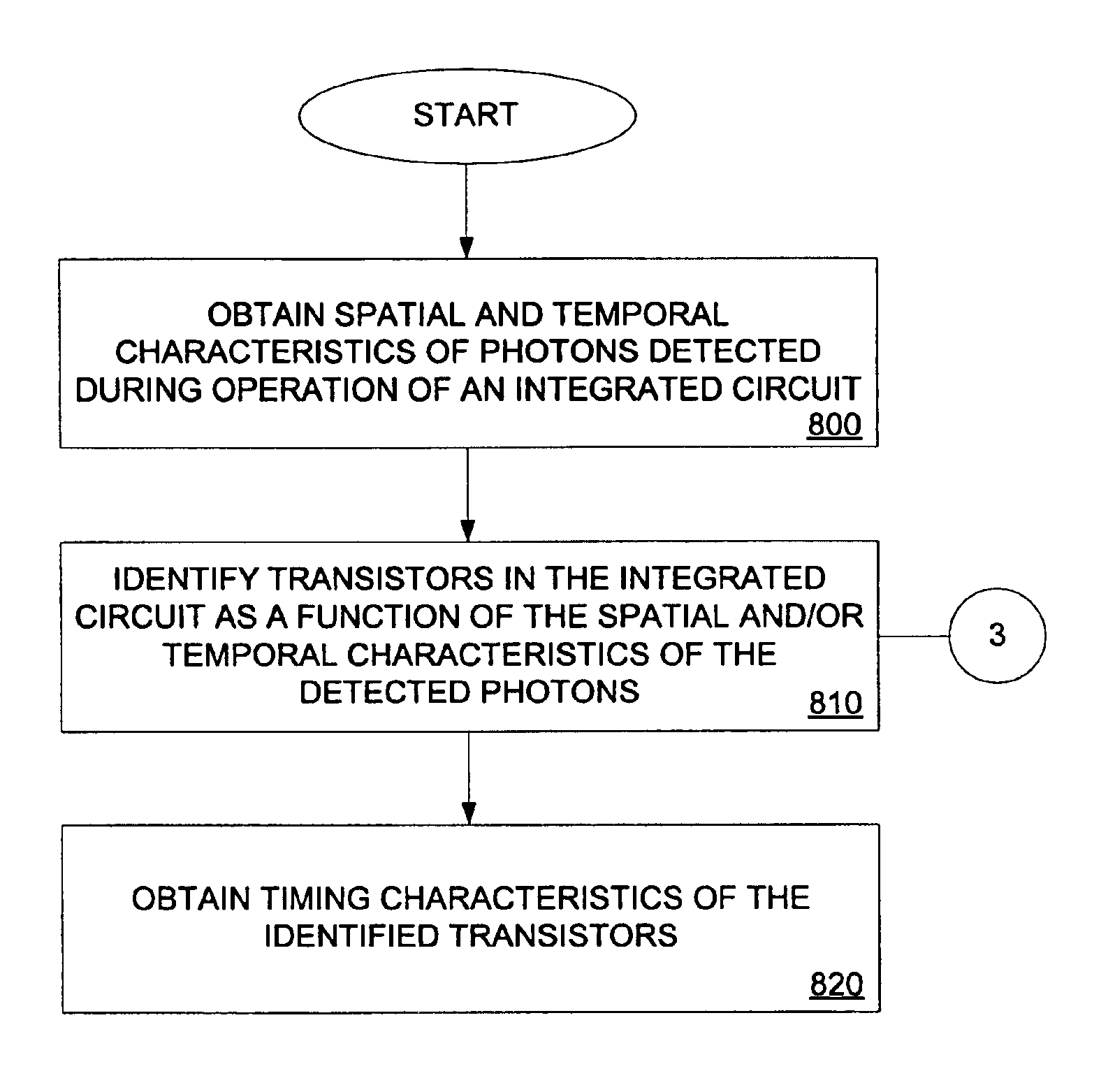
[0054]The present invention involves apparatuses and methods for analyzing photon emissions from an integrated circuit (IC) to identify transistors and extract timing information. Implementations of the present invention process photon emission data to rapidly discriminate between photons emitted by a transistor and photons attributable to background emissions. Generally, various aspects of the invention involve the correlation, grouping, or association of photons that have the same or similar spatial, temporal, spatial and temporal and other characteristics to discriminate between photons emitted from a transistor and randomly distributed background photon emissions. The discrimination between transistor photon emissions and background photon emissions can be used to identify a likelihood that photons were emitted from a transistor, identify a single transistor, identify many transistors in an entire IC or a portion of an IC, and extract timing information for the transistor or tra...


PUM


Abstract

A system, apparatus, and method for analyzing photon emission data to discriminate between photons emitted by transistors and photons emitted by background sources. The analysis involves spatial and/or temporal correlation of photon emissions. After correlation, the analysis may further involve obtaining a likelihood that the correlated photons were emitted by a transistor. After correlation, the analysis may also further involve assigning a weight to individual photon emissions as a function of the correlation. The weight, in some instances, reflecting a likelihood that the photons were emitted by a transistor. The analysis may further involve automatically identifying transistors in a photon emission image.

Description

FIELD OF THE INVENTION[0001]The present invention involves an apparatus and method for detecting photon emissions from one or more transistors, and more particularly involves an apparatus and method for rapidly discriminating between background photon emissions and transistor photon emissions, automatically identifying one or more transistors from photon emission data, and generating timing information for the identified transistors.BACKGROUND OF THE INVENTION[0002]The design and development of an integrated circuit (IC) oftentimes involves extensive testing to ensure that the IC functions correctly. It is common for an IC to include many millions of individual CMOS transistors in various logical arrangements to perform the functions of the IC. The physical size of CMOS transistors is continually shrinking, and gate length as small as 0.13 microns is becoming common. Testing such small discrete elements of an IC is difficult or impossible to perform by physically probing the IC. Mor...

Claims


Application Information

Patent Timeline
IPC IPC(8): G01R31/28G01R31/311
CPCG01R31/311G01R31/2656
Inventor DESPLATS, ROMAINCOUPANEC, PATRICIA LELO, WILLIAM K.PERDU, PHILIPPEKASAPI, STEVEN
Owner DCG SYST
Why Eureka
Try Eureka