Semiconductor pressure sensor and pressure sensing device

Inactive Publication Date: 2005-05-17
HITACHI LTD +1
View PDF11 Cites 51 Cited by
  • Summary
  • Abstract
  • Description
  • Claims
  • Application Information

AI Technical Summary

Benefits of technology

[0006]The present invention is intended to solve above-mentioned problems. Its object is to propose an etch channel sealing structure highly resistant to moisture and temporal change of t

Problems solved by technology

This will result in restrictions on the size of the etch channel,

Method used


Image

  • Semiconductor pressure sensor and pressure sensing device
  • Semiconductor pressure sensor and pressure sensing device
  • Semiconductor pressure sensor and pressure sensing device

Examples


Embodiment Construction

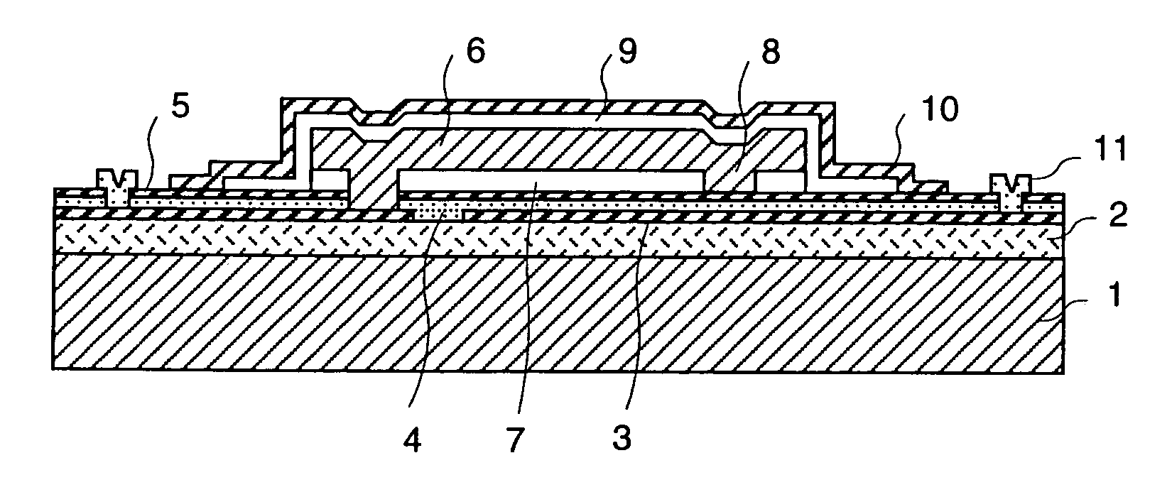
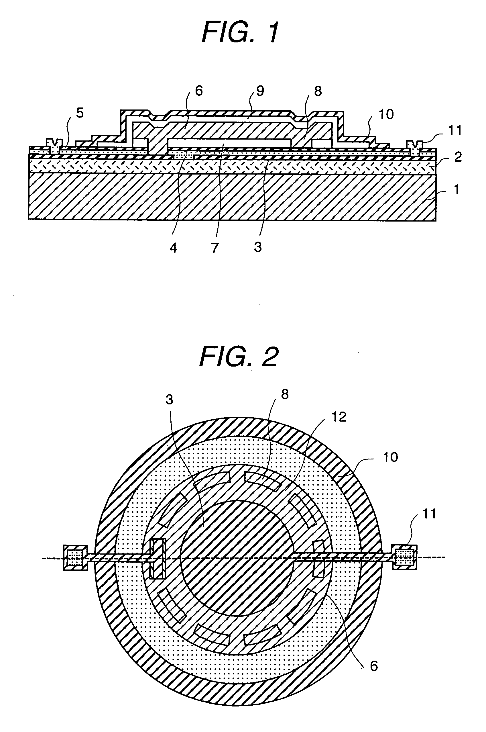
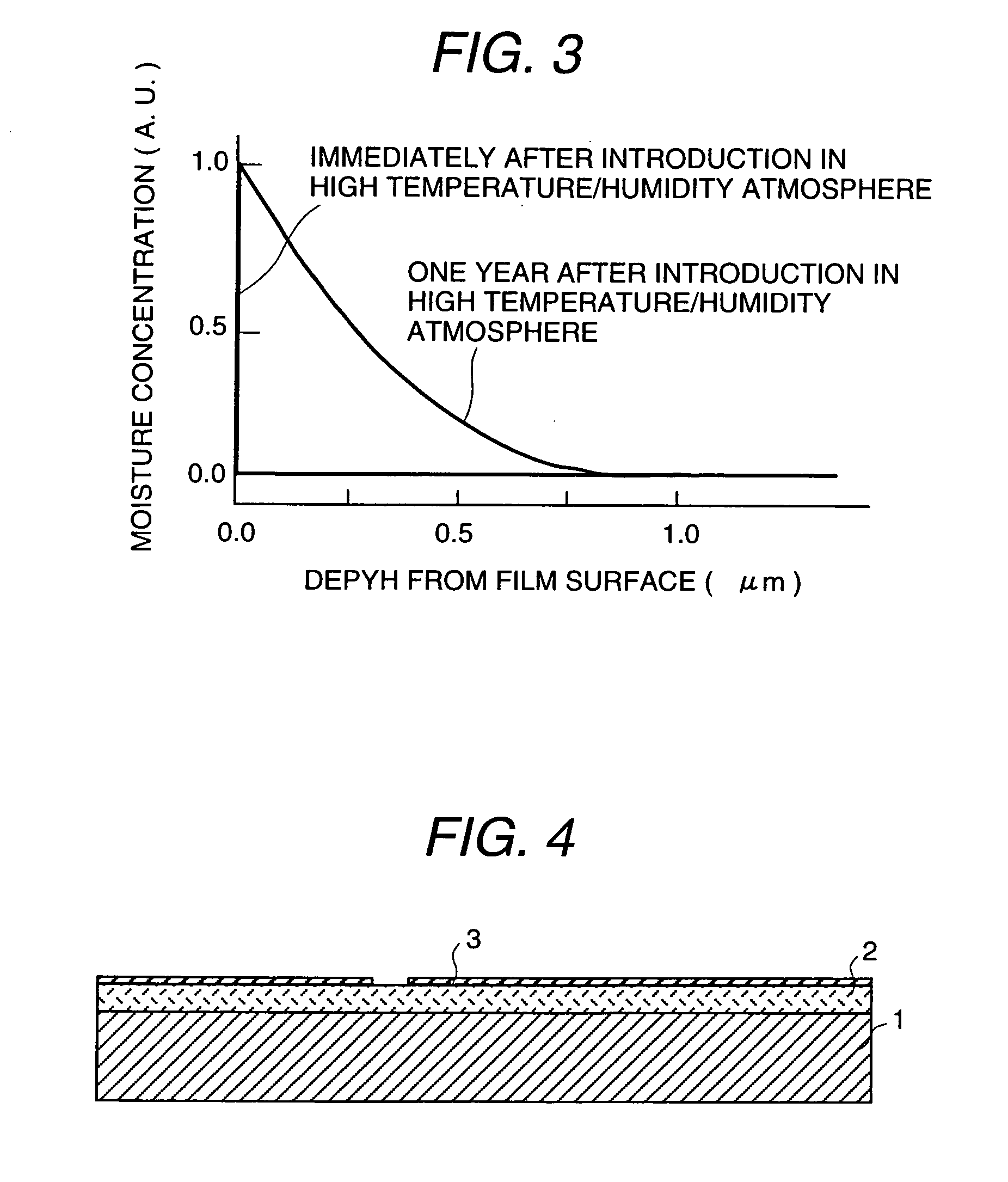
[0032]The following provides a detailed description of the present invention with reference to the embodiments given in the drawings: FIG. 1 is a cross sectional view representing an embodiment of a semiconductor pressure sensor according to the present invention, and FIG. 2 is a plan view thereof. The following describes the structure with reference to FIGS. 1 and 2. Monocrystal silicon substrate 1 is used for the substrate, and silicon oxide film 2 is formed on the surface thereof as an insulation layer. A fixed electrode 3 is formed on the silicon oxide film 2, and is made of polysilicon with phosphorus or other impurities dispersed thereon. Silicon oxide film 4 is formed on fixed electrode 3, and silicon nitride film 5 is formed on the surface thereof in order to protect the substrate surface in the sacrificial layer etching process to be discussed later and to avoid leak current on the substrate surface. Polysilicon diaphragm 6 with part of its periphery fixed on the silicon ni...


PUM


Abstract

The object of the present invention is to propose an etch channel sealing structure characterized by excellent impermeability to moisture and resistance to temporal change of the diaphragm in the pressure sensor produced according to the sacrificial layer etching technique, and to provide a pressure sensor characterized by excellent productivity and durability. After a very small gap is formed by the sacrificial layer etching technique, silicon oxide film is deposited by the CVD technique or the like, thereby sealing the etch channel. Further, impermeable thin film of polysilicon or the like is formed to cover the oxide film.
This allows an etch channel sealing structure to be simplified in the pressure sensor produced according to the sacrificial layer etching technique, and prevents entry of moisture into the cavity, thereby improving moisture resistance. Moreover, sealing material with small film stress reduces temporal deformation of the diaphragm.

Description

TECHNICAL FIELD[0001]The present invention relates to a semiconductor sensor having a micro-cavity structure and an actuator created based on the sacrificial layer etching technique, and particularly to an electrostatic capacitance semiconductor pressure sensor.BACKGROUND TECHNIQUE[0002]The prior art related to the present invention is disclosed in Japanese Application Patent Announcement Publication No. Hei 08-501156 as shown in FIG. 23, for example. This Patent describes the pressure sensor manufactured according to the sacrificial layer etching technique. Sacrificial layer etching is formed in the following process, for example: A sacrificial layer to be removed later is formed on the substrate in advance, and part of this layer is removed. A film remaining as a structure or anchor is formed thereon, and the end portion of the sacrificial layer is exposed to the outside. This portion is removed by etching, then a sensor and actuator are manufactured with the structural film. Or ...

Claims


Application Information

Patent Timeline
IPC IPC(8): B81B3/00B81B7/00G01L9/00G01L7/08H01L21/00
CPCB81C1/00293G01L9/0073G01L9/0042B81C1/00333B81B2201/0264B81B2203/0127B81C2203/0145
Inventor SATOU, SHINYASHIMADA, SATOSHIWATANABE, ATSUOONOSE, YASUOKURYU, SEIJIMIYAZAKI, ATSUSHIHORIE, JUNICHIMOMMA, NAOHIRO
Owner HITACHI LTD
Why Eureka
Try Eureka