Reconfigurable artificial magnetic conductor

a magnetic conductor and reconfigurable technology, applied in the direction of electrically short antennas, antenna details, antennas, etc., can solve the problems of inefficient radiating and too large thickness for many practical applications

Inactive Publication Date: 2005-05-24
TITAN AEROSPACE ELECTRONICS DIV +1
View PDF15 Cites 81 Cited by
  • Summary
  • Abstract
  • Description
  • Claims
  • Application Information

AI Technical Summary

Problems solved by technology

It will not radiate efficiently.
This thickness is too large for many practical applications.

Method used


Image

  • Reconfigurable artificial magnetic conductor
  • Reconfigurable artificial magnetic conductor
  • Reconfigurable artificial magnetic conductor

Examples


second embodiment

[0057]FIG. 11 and FIG. 12 illustrate a reconfigurable artificial magnetic conductor (RAMC) 1100. FIG. 11 is a top view of the RAMC 1100. FIG. 12 is a cross sectional view taken along line A—A in FIG. 11.

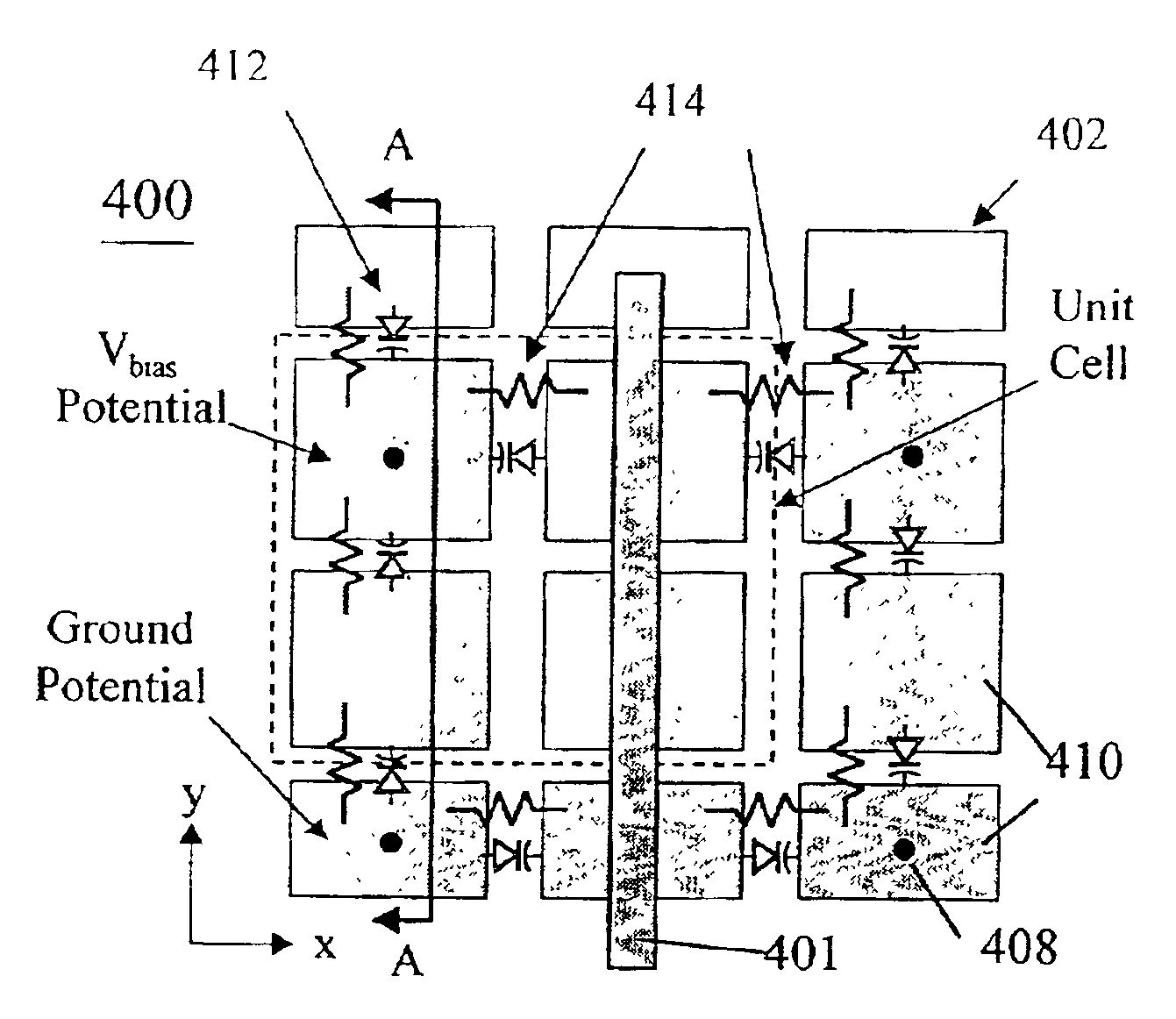
[0058]The RAMC 1100 includes a frequency selective surface (FSS) 1102, a spacer layer 1104 and a radio frequency (RF) backplane 1106. An antenna element 1103 is placed adjacent to the RAMC 1100 to form an antenna system. The backplane 1106 includes one or more bias voltage lines 1120 and a ground plane 1122. In one embodiment, the backplane is fabricated using printed circuit board technology to route the bias voltage lines. The spacer layer is pierced by conductive vias 1108. The conductive vias 1108 electrically couple bias control signals, communicated on the bias voltage lines 1120 of the conductive backplane, with adjacent conductive patches 1110 of the FSS 1102. The bias signals are labeled Vc1 and Vc2 in FIGS. 11 and 12. The bias control signals may be DC or AC signals or a co...

first embodiment

[0071]FIG. 17 is a cross sectional view of an artificial magnetic conductor (AMC) 1600 with a reduced number of vias 1608 in the spacer layer 1604. FIG. 20 is a top view of this same embodiment. In the embodiment of FIGS. 17 and 20, vias 1609 connect only to the lower or second patches 1612. The vias 1608 which in the embodiment of FIG. 16 had been associated with the upper or first patches 1610 are omitted. The vias 1609 are associated only with the second patches 1612. The vias 1609 may be electrically coupled with their associated patches or they may be separated from the patches 1612 by a dielectric. This can be achieved, for example, if the patches 1612 are annular with the via passing through the central region. Thus, in FIG. 17, the spacer layer of the AMC 1600 has conductive vias associated with some or all of only the first set of conductive patches formed on one side of the dielectric layer of the FSS.

[0072]Also, in FIG. 17, the vias 1609 are shown extending above the plan...


PUM


Abstract

An electronically reconfigurable artificial magnetic conductor (RAMC) includes a frequency selective surface (FSS) having an effective sheet capacitance which is variable to control resonant frequency of the RAMC. In one embodiment, the RAMC further includes a conductive backplane structure and a spacer layer separating the conductive backplane structure and the FSS. The spacer layer includes conductive vias extending between the conductive backplane structure and the FSS, and voltage variable capacitive circuit elements coupled with the FSS and responsive to bias voltages applied on one or more bias signal lines routed through the conductive backplane structure and the conductive vias.

Description

RELATED APPLICATIONS[0001]This application is related to U.S. Ser. No. 09 / 845,393, now U.S. Pat. No. 6,525,695, entitled RECONFIGURABLE ARTIFICIAL MAGNETIC CONDUCTOR USING VOLTAGE CONTROLLED CAPACITORS WITH COPLANAR RESISTIVE BIASING NETWORKS, which is commonly assigned with the present application and filed on even date herewith.FEDERALLY SPONSORED RESEARCH[0002]This invention was developed in part under DARPA Contract Number F19628-99-C-0080.BACKGROUND[0003]The present invention relates to the development of reconfigurable artificial magnetic conductor (RAMC) surfaces for low profile antennas. This device operates as a high-impedance surface over a tunable frequency range, and is electrically thin relative to the frequency of interest, λ.[0004]A high impedance surface is a lossless, reactive surface, realized as a printed circuit board, whose equivalent surface impedance is an open circuit which inhibits the flow of equivalent tangential electric surface currents, thereby approxim...

Claims


Application Information

Patent Timeline
Patent Type & Authority Patents(United States)
IPC IPC(8): H01Q3/46H01Q15/00H01Q3/00
CPCH01Q3/46H01Q15/008H01Q15/0066
Inventor MCKINZIE, III, WILLIAM E.SANCHEZ, VICTOR C.REED, MARKGARRETT, STEVEN L.
Owner TITAN AEROSPACE ELECTRONICS DIV
Why Eureka
Try Eureka