High voltage regulator for low voltage integrated circuit processes

a technology of integrated circuits and regulators, applied in the field of integrated circuits, can solve the problems of high voltage, inability to easily reduce to for the lower voltage tolerant process technologies, and loss of whatever data was in the ram, and achieve the effect of reducing external voltag

Inactive Publication Date: 2005-05-24
MICRON TECH INC
View PDF16 Cites 6 Cited by
  • Summary
  • Abstract
  • Description
  • Claims
  • Application Information

AI Technical Summary

Problems solved by technology

However, in many situations the externally supplied high voltage is fixed by past usage, convention, or industry specification and is unable to be easily reduced to for the lower voltage tolerant process technologies.
Most RAM is volatile, which means that it requires a steady flow of electricity to maintain its contents.
As soon as the power is turned off, whatever data was in RAM is lost.
A problem with external high voltage input in integrated circuits is that the modern process technologies are in many cases unable to tolerate the field or voltage level of the external high voltage input.
Additionally, as stated above, in many situations the externally supplied high voltage is fixed by past usage, convention, or industry specification and cannot be easily altered by the integrated circuit designer.
Voltage reduction circuits that utilize drain coupled back bias can suffer from reduced current flow because of the limited voltage available for generating the conducting carrier channel in the MOS transistor.
Also, the application of a rigidly fixed back bias cannot easily be adjusted for circuit needs and input voltages and / or reduce the available voltage for regulation.
An additional problem can be the size requirements of a voltage reduction circuit with multiple isolation wells.
A further issue is the possibility of a reverse bias condition when the external voltage input is pulled to ground and a voltage is being applied to the isolation well through the back bias / voltage regulator connection.

Method used


Image

  • High voltage regulator for low voltage integrated circuit processes
  • High voltage regulator for low voltage integrated circuit processes
  • High voltage regulator for low voltage integrated circuit processes

Examples


Embodiment Construction

[0023]In the following detailed description of the preferred embodiments, reference is made to the accompanying drawings that form a part hereof, and in which is shown by way of illustration specific preferred embodiments in which the inventions may be practiced. These embodiments are described in sufficient detail to enable those skilled in the art to practice the invention, and it is to be understood that other embodiments may be utilized and that logical, mechanical and electrical changes may be made without departing from the spirit and scope of the present invention. The following detailed description is, therefore, not to be taken in a limiting sense, and the scope of the present invention is defined only by the claims.

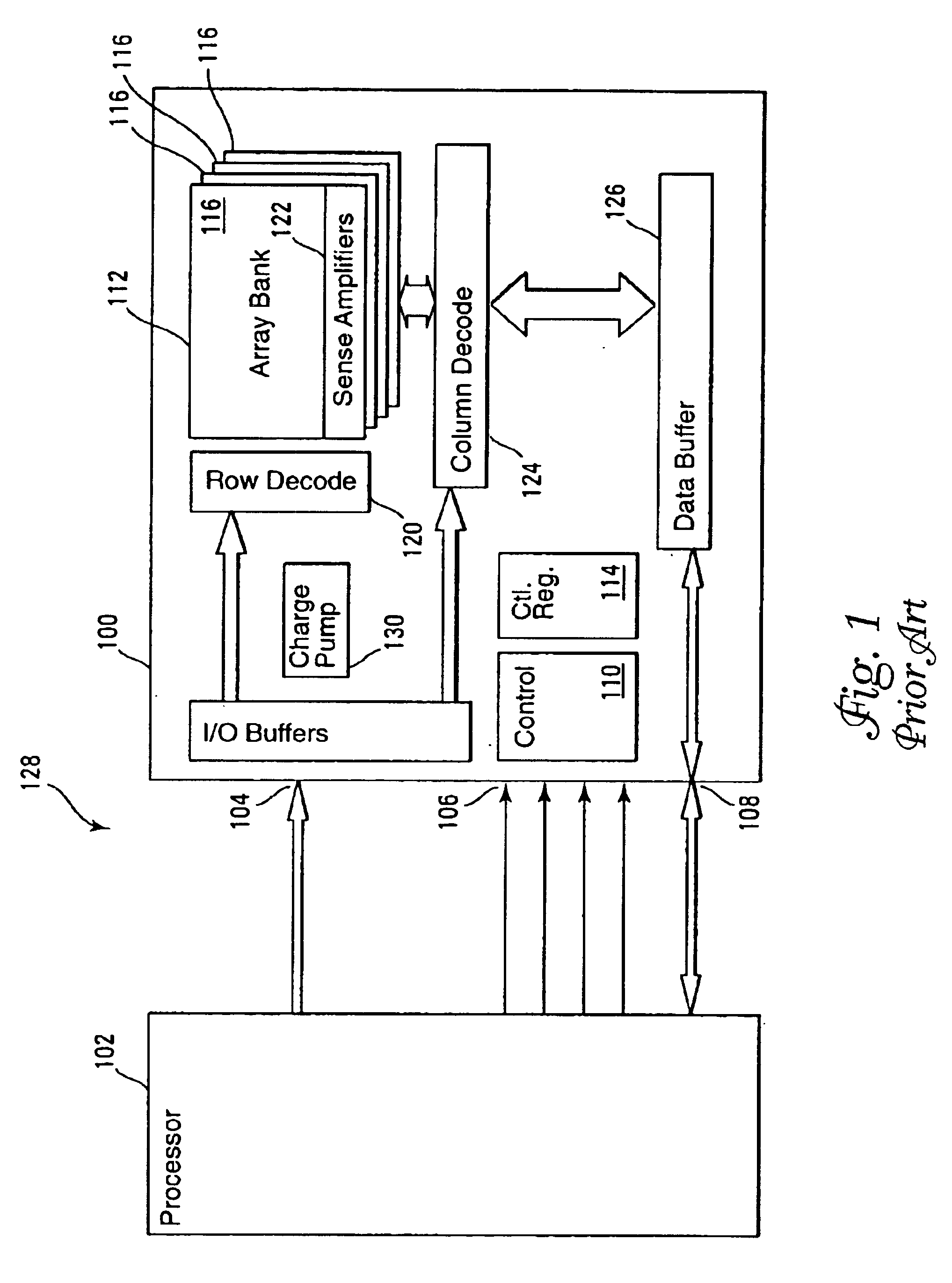
[0024]To deal with the above detailed issues of problems with high voltage regulation for integrated circuits and memories with low voltage processes, embodiments of the present invention utilize an improved voltage reduction circuit that applies an optimal, sep...


PUM


Abstract

An improved voltage reduction circuit and method is described that incorporates an independently controllable back bias voltage for increased gate / bulk fields in isolation well voltage reduction transistors that couple to and reduce external voltages that are too high for the integrated circuit process technology limits. The improved voltage reduction circuit and method allows for a higher overall available voltage and current flow for regulation by the circuit. Additionally, the improved voltage reduction circuit and method reduces voltage reduction circuit size by allowing for efficient implementation in a single isolation well. Furthermore, the improved voltage reduction circuit and method includes a back bias voltage control circuit that turns on and regulates the back bias voltage and avoids the problem of reverse bias conditions.

Description

RELATED APPLICATION[0001]This is a continuation application of U.S. patent application Ser. No. 10 / 184,756, filed Jun. 28, 2002 now U.S. Pat. No. 6,785,161, titled “HIGH VOLTAGE REGULAR FOR LOW VOLTAGE INTEGRATED CIRCUIT PROCESSES” and commonly assigned, the entire contents of which are incorporated herein by reference.TECHNICAL FIELD OF THE INVENTION[0002]The present invention relates generally to integrated circuits and in particular the present invention relates high voltage regulators and voltage reduction circuits utilized in low voltage integrated circuits.BACKGROUND OF THE INVENTION[0003]Most integrated circuits and memory devices are designed to operate using a specific voltage power supply, such as 5V+ / −10%, that their internal process technologies are designed to tolerate. In modern integrated circuits and memories, the need for higher voltage power supplies is reduced as the process feature sizes, such as transistors, are reduced and operating speeds increase. However, in...

Claims


Application Information

Patent Timeline
Patent Type & Authority Patents(United States)
IPC IPC(8): G11C5/14
CPCG11C5/146
Inventor PEKNY, THEODORE T.
Owner MICRON TECH INC
Why Eureka
Try Eureka