Semiconductor light emitting device having a silver p-contact

a silver p-contact, semiconductor technology, applied in the direction of semiconductor devices, basic electric elements, electrical appliances, etc., can solve the problems of reducing the amount of light that exits the device, wasting power at the junction, and wasting a large amount of effort in prior art devices to maximize, so as to achieve the effect of increasing the efficiency of light outpu

Inactive Publication Date: 2005-05-31
LUMILEDS
View PDF42 Cites 63 Cited by
  • Summary
  • Abstract
  • Description
  • Claims
  • Application Information

AI Technical Summary

Benefits of technology

[0011]It is a further object of the present invention to provide an LED with increased light output efficiency.

Problems solved by technology

A considerable amount of effort has been expended in prior art devices to maximize the light that is generated from the active layer per watt of drive power.
In either case, there is a voltage drop across the junction, and hence, power is wasted at the junction.
While increasing the size of the p-electrode increases the amount of light generated in the active region per watt of input power, it leads to a decrease in the amount of light that exits the device, since most of the light exiting the device must now pass through the p-electrode.
In addition, this transparent p-electrode is too thin for bonding to the electrical conductors used to deliver the power to the LED.
Hence, a significant amount of light is lost in the thicker bonding pad regions.
However, even with the best prior art designs, the amount of light exiting the LED is 50% of that generated in the active region.
As a result higher drive voltages are required to overcome the increased resistance, and efficiency drops.

Method used


Image

  • Semiconductor light emitting device having a silver p-contact
  • Semiconductor light emitting device having a silver p-contact
  • Semiconductor light emitting device having a silver p-contact

Examples


Embodiment Construction

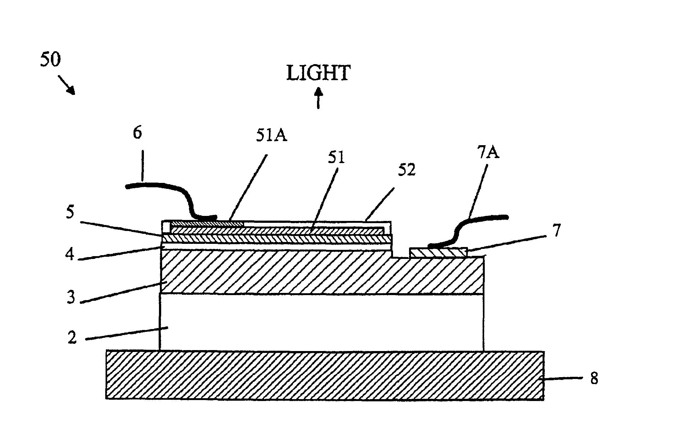
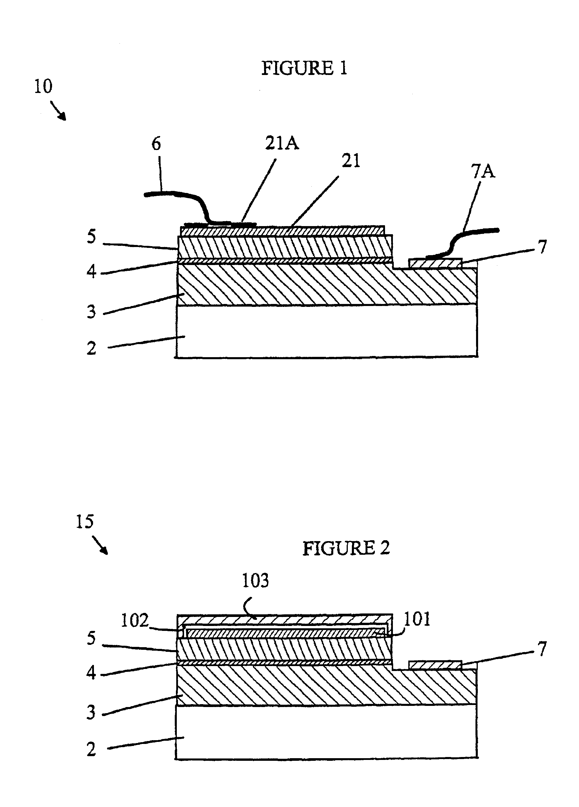
[0018]The present invention achieves its advantages by utilizing a silver-based p-electrode. An LED according to the present invention can be constructed with either a reflective p-electrode and a transparent substrate or a transparent p-electrode and a reflective substrate. Embodiments of the present invention utilizing a reflective p-electrode will be described first.

[0019]The light generated in the active region of the LED exits the LED through the substrate when a reflective p-electrode is utilized. Light exiting the active region in the direction of the p-electrode is reflected back toward the substrate by the reflective p-electrode. The p-electrode utilizes silver as the first metal layer in at least a part of the p-electrode. In an optoelectronic device according to the present invention, a silver layer is vapor-deposited on the p-type nitride semiconductor layer and functions as the p-electrode and as a mirror for reflecting light back toward the transparent substrate.

[0020]...


PUM


Abstract

A light emitting device is constructed on a substrate. The device includes an n-type semiconductor layer in contact with the substrate, an active layer for generating light, the active layer being in electrical contact with the n-type semiconductor layer. A p-type semiconductor layer is in electrical contact with the active layer, and a p-electrode is in electrical contact with the p-type semiconductor layer. The p-electrode includes a layer of silver in contact with the p-type semiconductor layer. A bonding layer is formed overlying the silver layer to make an electrical connection to the silver layer. The silver layer may be thin and transparent or thicker (greater than 20 nm) and reflective.

Description

CROSS-REFERENCE TO RELATED APPLICATIONS[0001]This application is a continuation of U.S. application Ser. No. 09 / 212,150, filed Dec. 15, 1998, now U.S. Pat. No. 6,194,793 entitled A Nitride Semiconductor Light Emitting Device Having A Silver P-Contact, incorporated herein by reference.FIELD OF THE INVENTION[0002]The present invention relates to light emitting electronic devices based on nitride semiconductors, and more particularly to an optoelectronic device that has improved optical and optoelectronic characteristics.BACKGROUND OF THE INVENTION[0003]The development of short wavelength light emitting devices is of great interest in the semiconductor arts. Such short wavelength devices hold the promise of providing increased storage density for optical disks as well as full-color displays and white light sources when used in conjunction with devices that emit light at longer wavelengths.[0004]One promising class of short wavelength light emitting devices is based on group III nitride...

Claims


Application Information

Patent Timeline
Patent Type & Authority Patents(United States)
IPC IPC(8): H01L33/00H01L33/40H01L33/42
CPCH01L33/40H01L33/42H01L2224/4847
Inventor KONDOH, YOUWATANABE, SATOSHIKANEKO, YAWARANAKAGAWA, SHIGERUYAMADA, NORIHIDE
Owner LUMILEDS
Why Eureka
Try Eureka