Surface-emitting semiconductor light device

a semiconductor light and surface-emitting technology, applied in the direction of semiconductor devices, basic electric elements, electrical equipment, etc., can solve the problems of low light output efficiency, low efficiency of increase, and low efficiency of light outpu

Inactive Publication Date: 2005-05-31
KK TOSHIBA
View PDF16 Cites 116 Cited by
  • Summary
  • Abstract
  • Description
  • Claims
  • Application Information

AI Technical Summary

Benefits of technology

[0020]FIG. 10 shows a plot of the light output efficiency versus the height of protrusions in the LED of FIG. 5;
[0021]FIG. 11 shows a plot of the light output efficiency versus the height of protrusions comparable in size with the emitted wavelength;
[0022]FIG. 12 shows a plot of the light output efficiency versus the refractive index when the surface of the antireflection film is roughened;
[0023]FIG. 13 shows a plot of the light output efficiency versus the refractive index when the surface of the antireflection film is made smooth;

Problems solved by technology

However, even with this method, an increase in the efficiency is low, of the order of 20%.
Thus, the conventional LEDs that are packaged with transparent resin material suffer from the problem that the light output efficiency is low.
This problem is common to surface-emitting LDs.

Method used


Image

  • Surface-emitting semiconductor light device
  • Surface-emitting semiconductor light device
  • Surface-emitting semiconductor light device

Examples


first embodiment

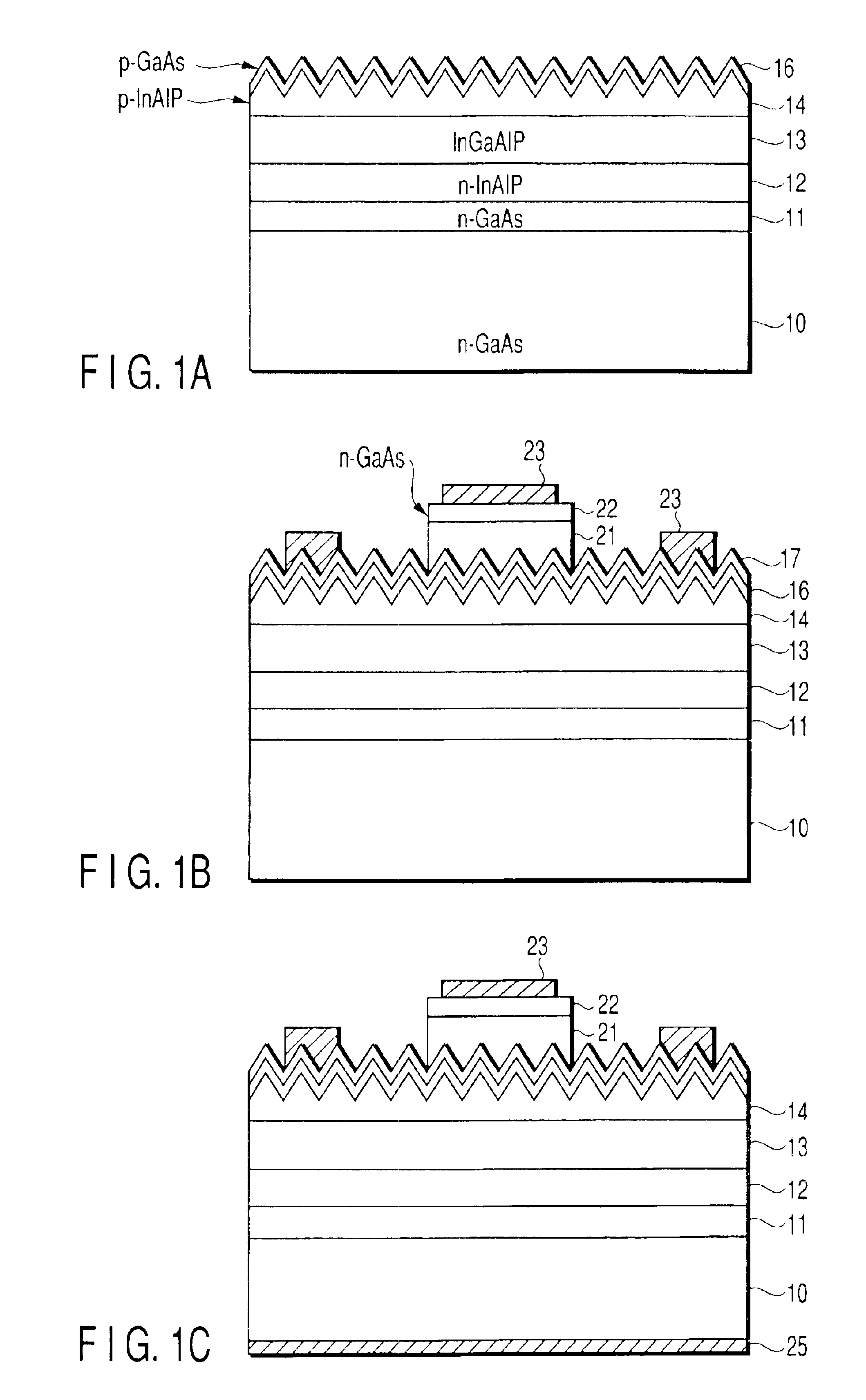
[0028]FIGS. 1A, 1B and 1C are cross-sectional views, in the order of steps of manufacture, of a green LED according to the present invention.

[0029]First, as shown in FIG. 1A, onto an n-type GaAs substrate 10 of 250 μm in thickness, an n-type GaAs buffer layer 11 of 0.5 μm in thickness is grown by means of metal-organic CVD (MOCVD) using AsH3 as a group V element source gas. After that, by means of MOCVD using PH3 as a group V element source gas and under conditions of a PH3 partial pressure of 200 Pa and a total pressure of 5×10³ Pa, an n-type In0.5Al0.5P cladding layer 12 of 0.6 μm in thickness and an undoped In0.5(Ga0.55Al0.45)0.5P active layer 13 of 1.0 μm in thickness are grown in sequence.

[0030]Subsequently, a p-type In0.5Al0.5P cladding layer 14 of 1.0 μm in thickness is grown by means of MOCVD with the PH3 partial pressure reduced to 10 Pa and the total pressure kept at 5×10³ Pa. After that, a p-type GaAs contact layer 16 of 0.1 μm in thickness is grown by means of MOCVD usin...

second embodiment

[0043][Second Embodiment]

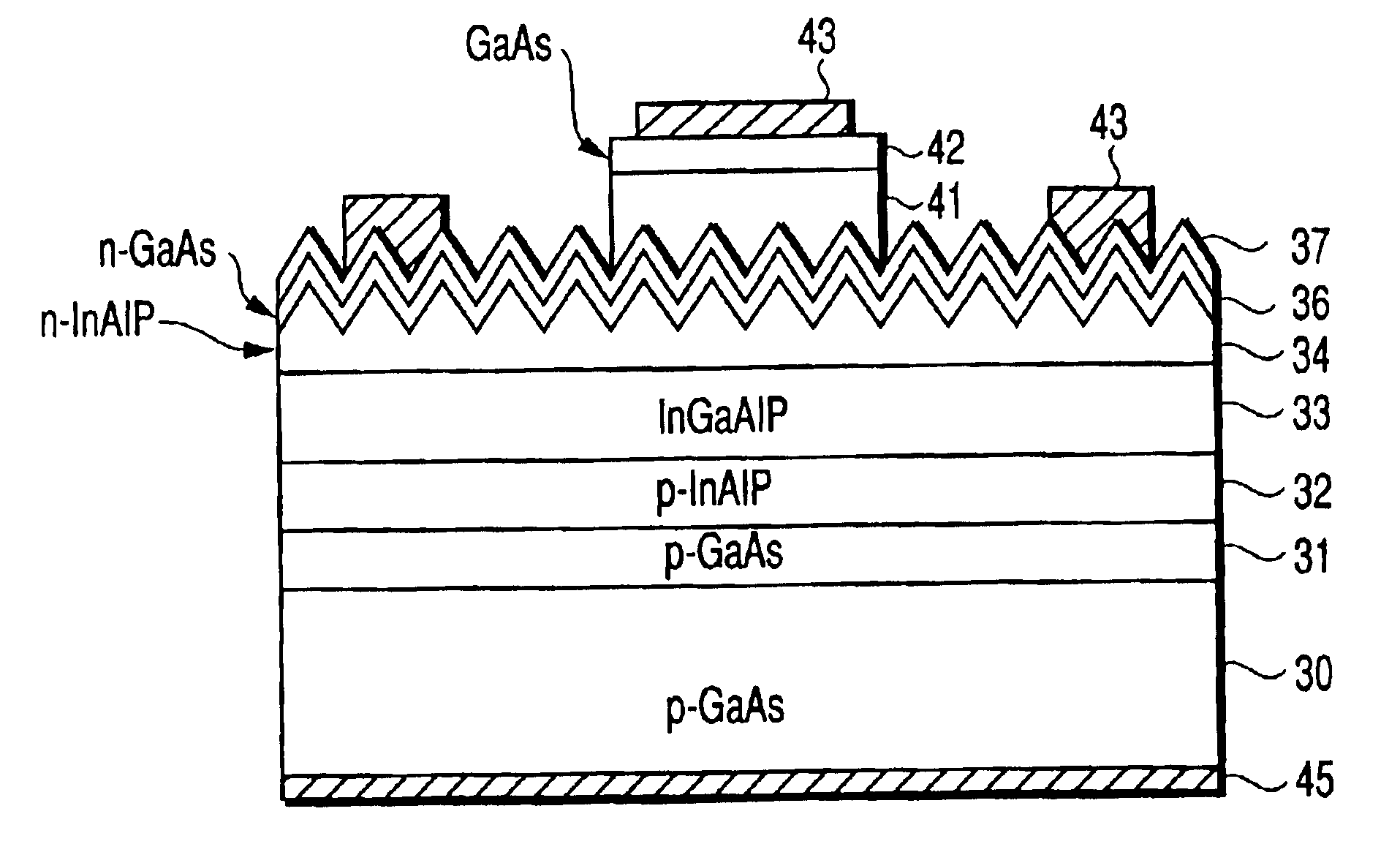
[0044]Referring now to FIG. 5, there is illustrated, in sectional view, the structure of a green LED according to a second embodiment of the present invention.

[0045]In the second embodiment, each of grown layers is opposite in conductivity type to a corresponding one of the grown layers in the first embodiment and the basic structure and the method of manufacture of the LED remain unchanged from those of the first embodiment.

[0046]Onto a p-type GaAs substrate 30 are sequentially grown by means of MOCVD a p-type GaAs buffer layer 31 of 0.5 μm in thickness, a p-type In0.5Al0.5P cladding layer 32 of 0.6 μm in thickness, an undoped InGaAlP active layer 33 of 1.0 μm in thickness, an n-type In0.5Al0.5P cladding layer 34 of 1.0 μm in thickness, and an n-type GaAs contact layer 36 of 0.1 μm in thickness. A transparent ITO film 37 is then formed on the contact layer 36 by means of sputtering techniques.

[0047]As in the first embodiment, in growing the n-type InAlP cla...

third embodiment

[0050][Third Embodiment]

[0051]FIGS. 6A and 6B are sectional views, in the order of steps of manufacture, of a green LED according to a third embodiment of the present invention.

[0052]First, as shown in FIG. 6A, onto an n-type GaAs substrate 50 of 250 μm in thickness are sequentially grown by means of MOCVD an n-type In0.5Al0.5P cladding layer 12 of 0.6 μm in thickness, an undoped In0.5(Ga0.55Al0.45)0.5P active layer 53 of 1.0 μm in thickness, a p-type In0.5Al0.5P cladding layer 54 of 1.0 μm in thickness, an n-type InGaP current diffusing layer 55 of 3.0 μm in thickness, and a p-type GaAs contact layer 56 of 0.1 μm in thickness. For epitaxial growth of these layers, the MOCVD techniques are used as in the first embodiment.

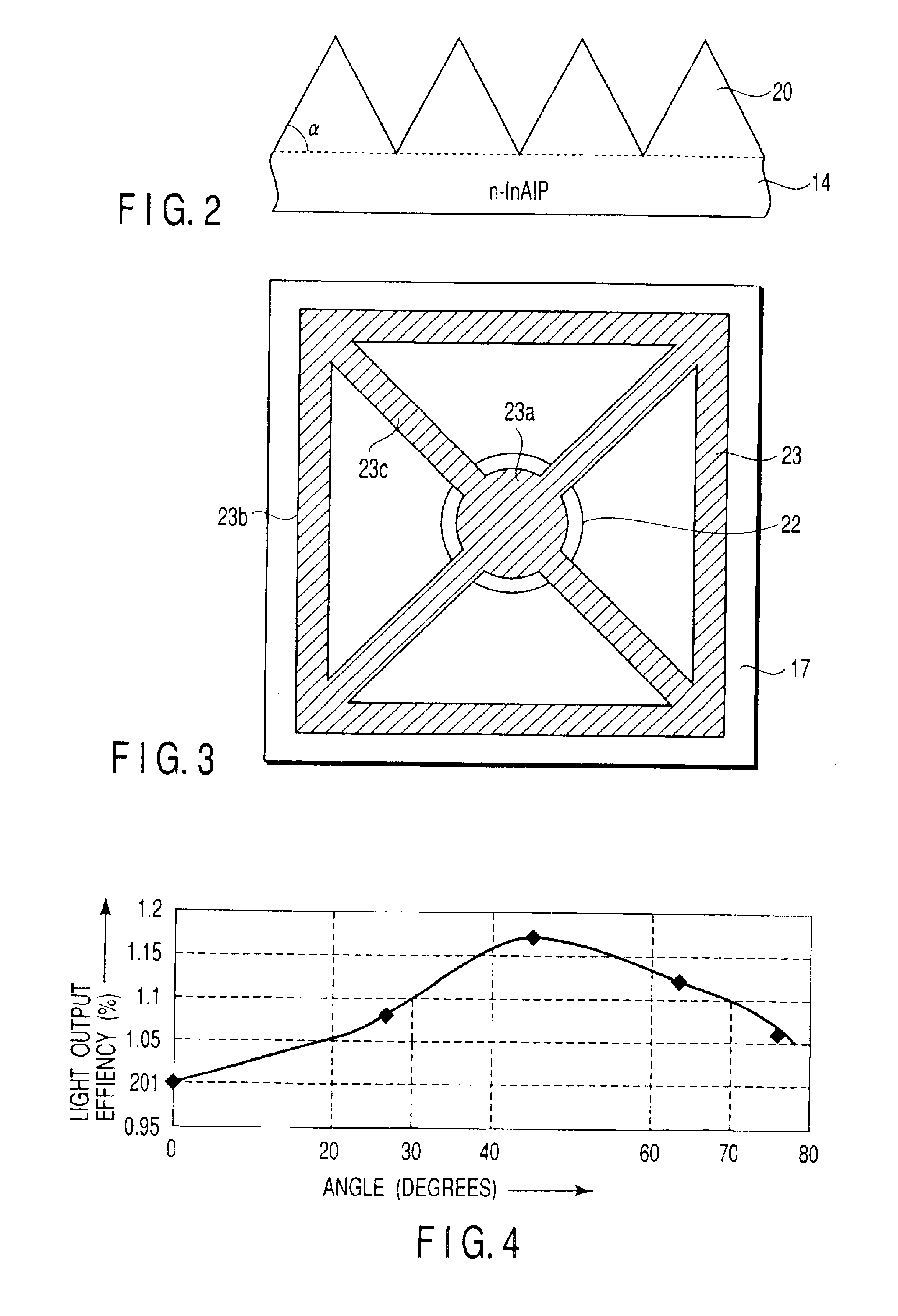
[0053]Next, an annealing step is performed at a temperature equal to or higher than the epitaxial temperature (not lower than 600° C.) in order to change the epitaxial surface topography. Thereby, the surface of the current diffusing layer 55 becomes roughened to fo...


PUM


Abstract

A semiconductor light emitting device is disclosed in which a semiconductor multilayer structure including a light emitting layer is formed on a substrate and light is output from the opposite surface of the semiconductor multilayer structure from the substrate. The light output surface is formed with a large number of protrusions in the form of cones or pyramids. To increase the light output efficiency, the angle between the side of each protrusion and the light output surface is set to between 30 and 70 degrees.

Description

CROSS-REFERENCE TO RELATED APPLICATIONS[0001]This application is based upon and claims the benefit of priority from the prior Japanese Patent Applications No. 2001-191724, filed Jun. 25, 2001; and No. 2001-297042, filed Sep. 27, 2001, the entire contents of both of which are incorporated herein by reference.BACKGROUND OF THE INVENTION[0002]1. Field of the Invention[0003]The present invention relates to a semiconductor light emitting diode, such as a light emitting diode (LED) or a laser diode (LD). More specifically, the present invention relates to a semiconductor light emitting device having its light output surface made rough.[0004]2. Description of the Related Art[0005]Conventionally, a high intensity LED has been fabricated by forming a double-heterostructure light emitting region on a semiconductor substrate and then forming a current diffusing layer on the light emitting region. For this reason, packaging the high intensity LED with a resin results in a structure in which the...

Claims


Application Information

Patent Timeline
Patent Type & Authority Patents(United States)
IPC IPC(8): H01L33/00H01L33/20H01L33/22H01L33/38H01L33/44
CPCH01L33/44H01L33/22H01L33/20H01L33/38
Inventor YOSHITAKE, SHUNJISEKIGUCHI, HIDEKIYAMASHITA, ATSUKOTAKIMOTO, KAZUHIROTAKAHASHI, KOICHI
Owner KK TOSHIBA
Why Eureka
Try Eureka