Resin molded semiconductor device on a lead frame and method of manufacturing the same

a semiconductor device and lead frame technology, applied in semiconductor devices, semiconductor/solid-state device details, electrical apparatus casings/cabinets/drawers, etc., can solve the problems of reducing the contact area between the lead frame and the sealing resin as a whole, lowering the reliability of a product, and reducing the adhesiveness. , to achieve the effect of stabilizing connection, enhancing the effect of absorbing stress and further improving the anchoring effect of the sealing resin

Inactive Publication Date: 2005-05-31
TESSERA ADVANCED TECH
View PDF37 Cites 20 Cited by
  • Summary
  • Abstract
  • Description
  • Claims
  • Application Information

AI Technical Summary

Benefits of technology

[0012]In this way, the lead frame is subjected to an upsetting process so that the die pad portion is located at a position higher than the inner lead portions. Therefore, the sealing resin of a thickness corresponding to the step difference of the upsetting exists below the die pad portion, the adhesiveness between the lead frame and the sealing resin can be improved, and the reliability of a product can be maintained. Even when both the faces, or the upper and lower faces of the lead frame are resin-molded, the thickness of the resin of the lower face is equal to a value corresponding to the step difference of the upsetting. Consequently, the thinning can be realized.
[0029]In this way, when the terminals of the semiconductor chip are to be electrically connected to the inner lead portions by the thin metal wires, the connection is performed while connecting portions of the thin metal wires on the side of the inner lead portions are disposed between the groove portions. Therefore, stress due to the structure in which the single face of the lead frame is molded by the sealing resin is absorbed by the groove portions, and does not act on an area between the groove portions. Consequently, the connecting portions of the thin metal wires are not broken, and stable connection is enabled. In this case, when two or more groove portions are disposed and the thin metal wires are connected to an area between the groove portions, the effect of absorbing stress can be enhanced. Moreover, the anchoring effect to the sealing resin can be further improved, and stress acting on a lead portion of a product can be further relaxed by the plural groove portions, and the effect of preventing leads and the thin metal wires from peeling off is enhanced.

Problems solved by technology

Even when a tapered shape is formed in an inner lead portion, therefore, the contact area between the lead frame and the sealing resin is reduced as a whole, thereby producing a problem in that the adhesiveness is impaired and the reliability of a product is lowered.
Since such a device has a structure in which substantially only the single face of the lead frame is resin-molded, there are further problems in that the semiconductor chip is adversely affected by stress of the sealing resin, and that package crack occurs in the sealing resin.
When the inner lead portions are connected to the semiconductor chip by thin metal wires and single-side molding is performed, there arises a further problem in that, because of stress in the single-side molding structure, a load due to the stress acts on the inner lead portions which are connected by thin metal wires, and the connecting portions are broken, with the result that a connection failure occurs.

Method used


Image

  • Resin molded semiconductor device on a lead frame and method of manufacturing the same
  • Resin molded semiconductor device on a lead frame and method of manufacturing the same
  • Resin molded semiconductor device on a lead frame and method of manufacturing the same

Examples


Embodiment Construction

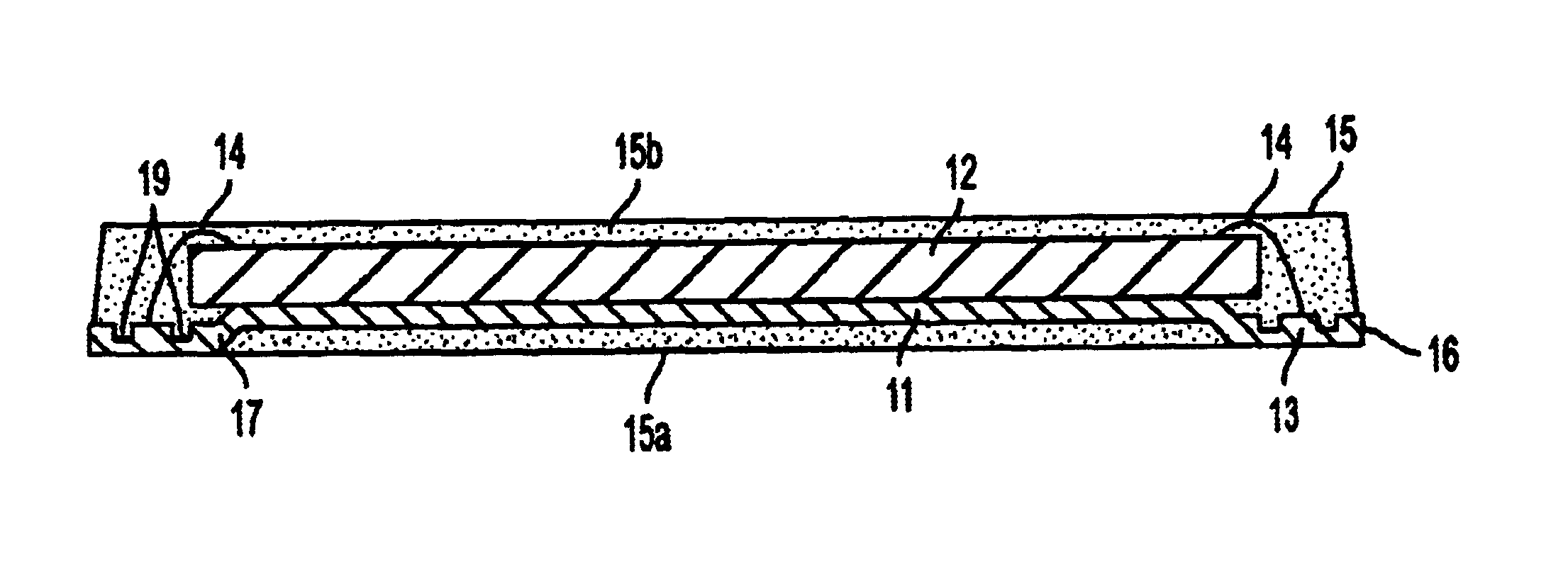
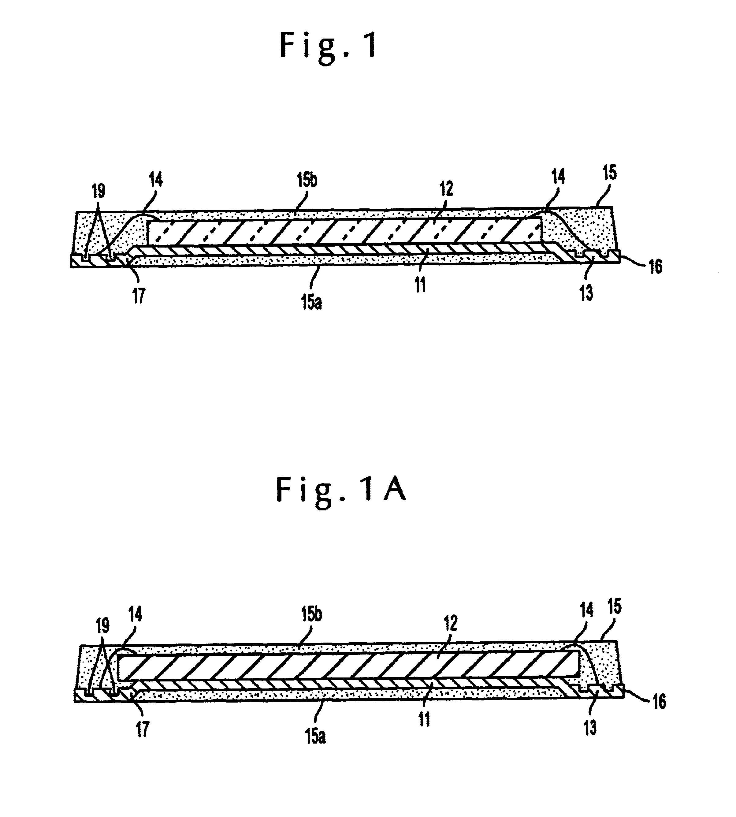
[0031]A resin molded type semiconductor device of an embodiment of the invention will be described with reference to FIGS. 1 to 4.

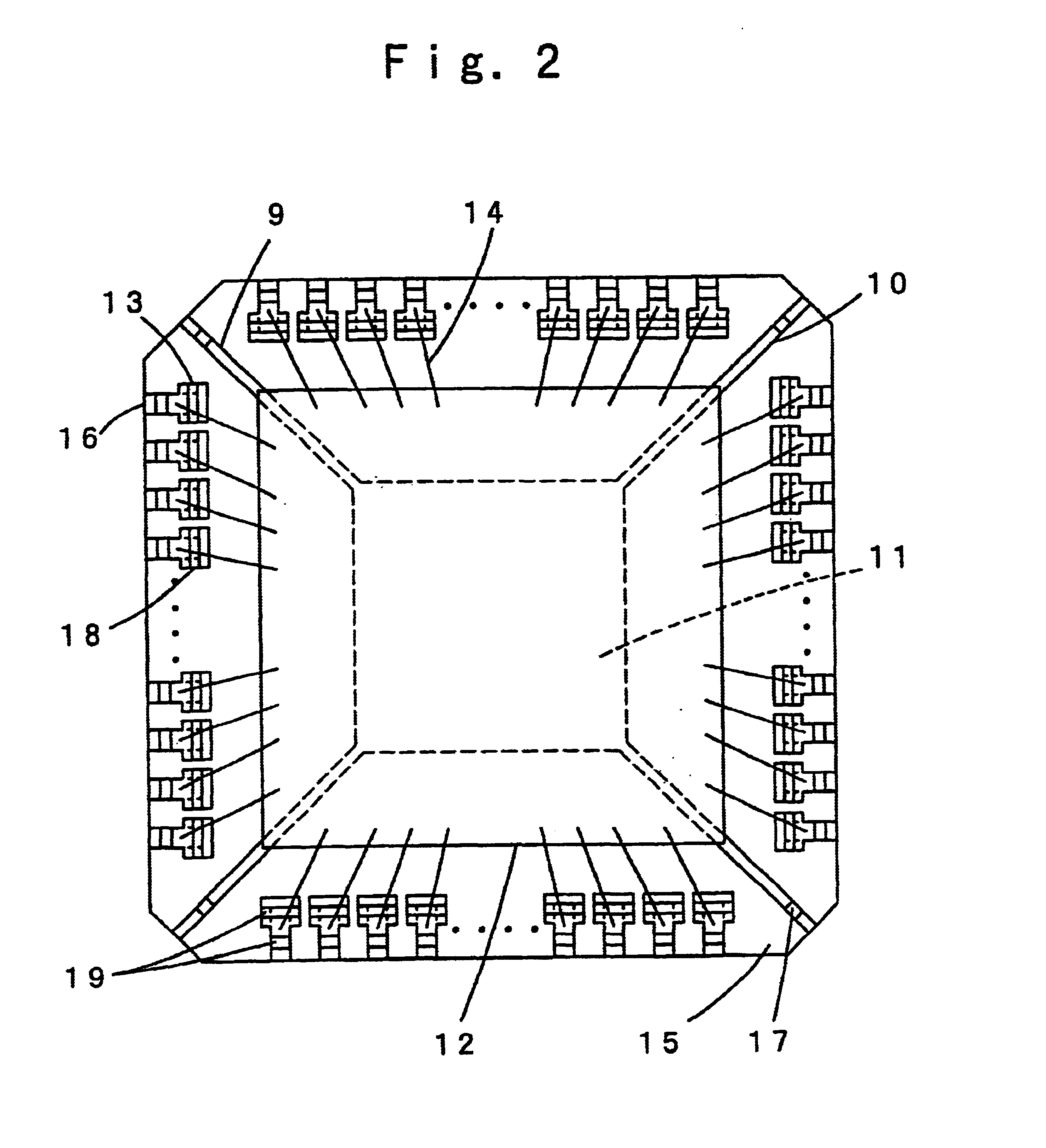
[0032]FIG. 1 is a section view of the resin molded type semiconductor device of the embodiment of the invention, FIG. 2 is a plan view of the device, FIG. 3 is an enlarged section view showing an inner lead portion of the device, FIG. 4(a) is an enlarged plan view showing a tip end of the inner lead portion, FIG. 4(b) is a left side view, and FIG. 4(c) is a front view. In FIG. 2, for the sake of convenience, the plan view is a view which is obtained by partially removing away a sealing resin, in order to show the internal structure. In the figure, broken lines show a die pad portion and part of suspension leads.

[0033]As shown in FIGS. 1 and 2, the resin molded type semiconductor device comprises: a semiconductor chip 12 which is mounted on a die pad portion 11 of a lead frame 9 and serving as a supporting portion of the semiconductor chip 12 supported by ...


PUM


Abstract

A resin molded type semiconductor device has: a semiconductor chip (12) which is mounted on a die pad portion (11) of a lead frame (9); thin metal wires (14) which connect terminals of the semiconductor chip (12) to inner lead portions (13) of the lead frame (9); and a sealing resin (15), and the lead frame (9) is subjected to an upsetting process so that a supporting portion (11) is located at a position higher than the inner lead portions (13). Since the sealing resin of a thickness corresponding to the step difference of the upsetting exists below the supporting portion, the adhesiveness between the lead frame and the sealing resin can be improved, and high reliability and thinning are realized. Since at least one groove portion is disposed in the surface of each of the inner lead portions (13), the anchoring effect to the sealing resin (15), stress acting on a lead portion of a product, and stress to the thin metal wires (14) can be relaxed, and leads and the thin metal wires can be prevented from peeling off.

Description

TECHNICAL FIELD[0001]The invention relates to a resin molded type semiconductor device in which a semiconductor chip is mounted on a lead frame and the outer periphery of the semiconductor chip, particularly, the upper face of the semiconductor chip is molded by a sealing resin, and also to a method of manufacturing the semiconductor device.BACKGROUND ART[0002]Recently, as the density of board mounting advances, semiconductor products which are to be mounted on a board are requested to be miniaturized and thinned. In order to realize miniaturization and thinning, the TAB mounting technique using a resin tape has been developed. In a development of a thin semiconductor product using a lead frame, a resin molded type semiconductor device of the single-side molding type in which a semiconductor chip is mounted on a lead frame and the mounting face is molded by a sealing resin has been developed.[0003]Hereinafter, a resin molded type semiconductor device of the prior art will be describ...

Claims


Application Information

Patent Timeline
Patent Type & Authority Patents(United States)
IPC IPC(8): H01L23/495H01L23/28H01L23/31H01L23/48H01L23/50
CPCH01L23/3107H01L23/49541H01L23/49548H01L2224/48091H01L2224/48247H01L2224/49171H01L2924/01057H01L24/49H01L24/48H01L2924/00014H01L2924/00H01L2224/451H01L2924/181H01L2924/00012H01L2224/45099H01L2224/45015H01L2924/207H01L23/31
Inventor MINAMIO, MASANORIKONISHI, SATORUMORISHITA, YOSHIHIKOYAMADA, YUICHIROITOH, FUMITO
Owner TESSERA ADVANCED TECH
Why Eureka
Try Eureka