Phase interpolator and receiver for adjusting clock phases into data phases
a phase interpolator and clock phase technology, applied in the direction of pulse manipulation, logic circuit coupling/interface arrangement, pulse technique, etc., can solve problems such as data read error, data voltage fluctuation, data read error,
- Summary
- Abstract
- Description
- Claims
- Application Information
AI Technical Summary
Problems solved by technology
Method used
Image
Examples
first embodiment
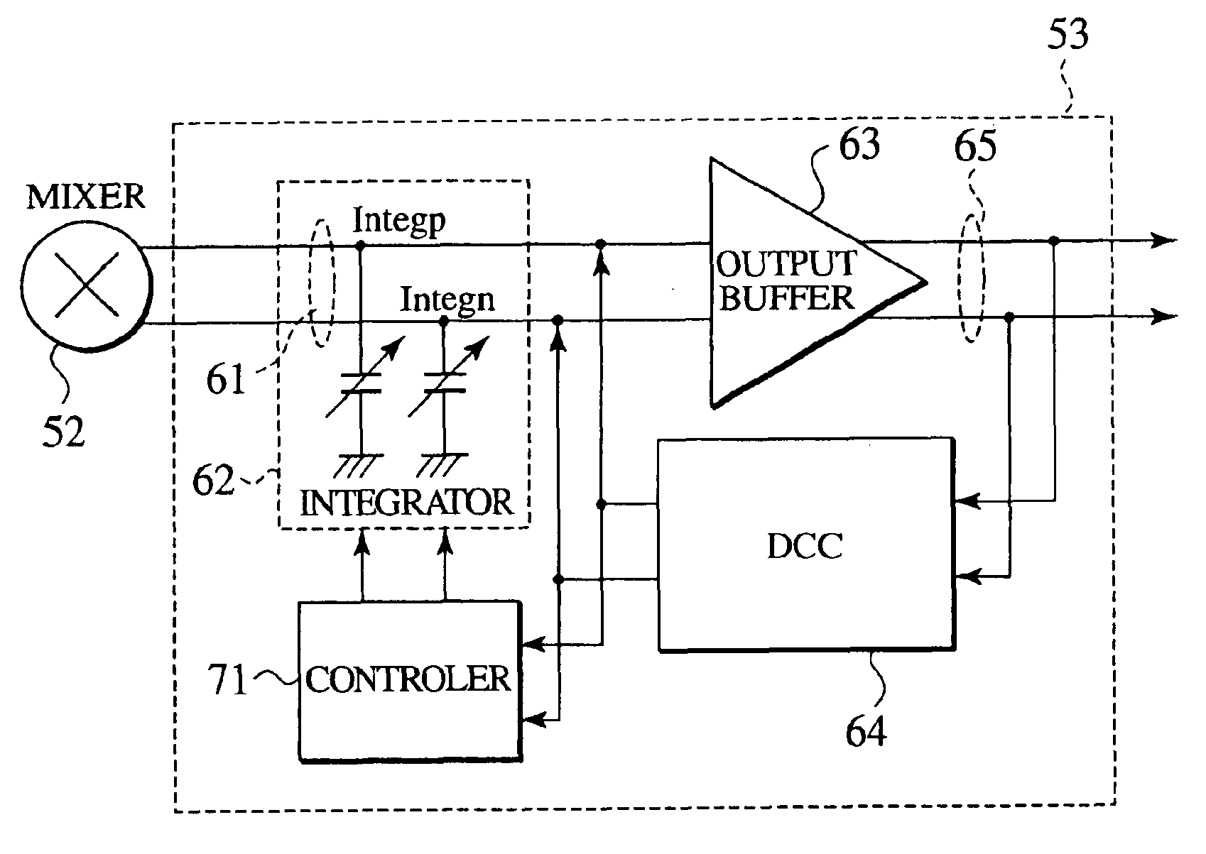
[0035]FIG. 4 is a circuit diagram showing examples of the controller 71 and integrator 62 according to the present invention. The controller 71 has an operational amplifier 21, a capacitor 12, and an inverter 13. The integrator 62 has an NMOS transistor 14a connected to one (61a) of the differential clock signals, a capacitor 15aconnected to the NMOS transistor 14a, an NMOS transistor 14bconnected to the other (61b) of the differential clock signals, and a capacitor 15b connected to the NMOS transistor 14b. The operational amplifier 21 finds a difference between the positive signal 61a or Integp and the negative signal 61b (an inverted signal due to the CML) or Integn. The operational amplifier 21 then compares the found differential voltage with a reference signal 17 or Vref. If the differential voltage is smaller than the reference signal Vref, the operational amplifier 21 provides a detected signal. Here, the capacitor 12 is able to prevent a switching of the inverter 13 upon fir...
second embodiment
[0040]FIG. 8 is a circuit diagram showing examples (71a, 62a) of the controller 71 and integrator 62 according to the present invention. Compared with FIG. 4, the controller 71a has two operational amplifiers 21a and 21bthat receive different reference signals Vref1 and Vref2, respectively. The operational amplifier 21a finds a difference between the signals Integp and Integn and compares the differential voltage with the reference signal Vref1. If the differential voltage is smaller than the reference signal Vref1, a predetermined amount of charge is accumulated in a capacitor 12a. On the other hand, the operational amplifier 21b finds a difference between the signals Integp and Integn and compares the differential voltage with the reference signal Vref2. If the differential voltage is smaller than the reference signal Vref2, a predetermined amount of charge is accumulated in a capacitor 12b. Based on these different standards, the operational amplifiers 21a and 21b turn off NMOS t...
third embodiment
[0041]FIG. 9 is a circuit diagram showing examples (71b, 62b) of the controller 71 and integrator 62 according to the present invention. The controller 71b has an operational amplifier 22a that receives the signals Integp, Integn, and Vref1, an operational amplifier 22b for receiving the signals Integp, Integn, and Vref2, a delay circuit 25 for delaying the output of the operational amplifier 22b, a flip-flop (FF) for receiving the output of the delay circuit 25 at a clock input terminal and the output of the operational amplifier 22a at an input terminal, an inverter 26 for inverting the output of the delay circuit 25, a flip-flop 24 for receiving the output of the inverter 26 at a clock input terminal and the output of the flop-flop 23 at an input terminal, and a NAND gate 27 for receiving the outputs of the flip-flops 23 and 24 and providing a NAND of the received signals. The controller 71b is an example of a counter circuit. The operational amplifier 22a receives the signals In...
PUM
 Abstract
Description
Claims
Application Information


