Liquid crystal display device and method for driving the same

a liquid crystal display and super twisted nematic technology, applied in the direction of electric digital data processing, instruments, computing, etc., can solve the problems of high level of induced distortion in scanning voltage, inability to completely correct differences in induced distortion crosstalk in lateral direction along row electrodes, and significant decrease in display quality, so as to reduce correction errors, suppress the effect of induced distortion crosstalk and lateral differences in induced distortion crosstalk

Inactive Publication Date: 2005-05-31
SHARP KK
View PDF11 Cites 46 Cited by
  • Summary
  • Abstract
  • Description
  • Claims
  • Application Information

AI Technical Summary

Benefits of technology

[0049]Thus, the invention described herein makes possible the advantages of providing: (1) an LCD device and a driving method therefor for correcting and smoothing differences in induced distortion crosstalk in a lateral direction along a row electrode, in which, in the device and method of the present invention, the correction can be achieved without an increase in circuit scale and independent of column drivers and therefore, the induced distortion crosstalk can be optimally corrected with small errors and high precision; and (2) an LCD device and a driving method therefor for correcting the above-described induced distortion crosstalk and at the same time, optimally correcting blunt waveform crosstalk and a gradation phenomenon.
[0051]In the present invention, a correction voltage for correcting a change in an effective voltage value caused by distortion of a scanning voltage waveform due to a change in signal voltage is applied to each column electrode in a correction period. In this case, the correction period which is equal to m horizontal scanning periods is provided in L horizontal scanning periods where L is an integer greater than or equal to 2 and m is an integer more than 0 and less than L. Thereby, display irregularity caused by the induced distortion crosstalk can be suppressed. Further, in the present invention, a means for generating a correction voltage which is varied every one or more column electrodes is provided. Therefore, differences in the induced distortion crosstalk in a lateral direction along row electrodes as well as the gradation phenomenon can be suppressed. Correction amounts corresponding to (L−m) horizontal scanning periods can be accumulated, thereby reducing a correction error.
[0052]Further, in the present invention, a means is provided for adding or subtracting an error between an increment or decrement of the correction voltage and an increment or decrement of an effective voltage value to or from a correction voltage which will be applied in the next correction period, thereby further improving the precision of correction.

Problems solved by technology

Conventional STN liquid crystal display (LCD) devices have a problem that as display capacity, such as liquid crystal capacity is increased, display irregularity depending on display patterns emerges, leading to a significant decrease in display quality.
Specifically, when the waveforms of signal voltages applied to a number of column electrodes are simultaneously changed, a high level of induced distortion occurs in scanning voltage, so that an effective voltage value applied to each pixel is increased or decreased to be shifted from an intended effective voltage value.
For this reason, differences in the induced distortion crosstalk in a lateral direction along a row electrode cannot be completely corrected.
Thus, the above-described induced distortion crosstalk cannot be optimally corrected.
In practice, circuit scale is disadvantageously increased so that differences in the above-described induced distortion crosstalk can be corrected and smoothed.
The differences in the induced distortion crosstalk in the lateral direction along a row electrode cannot be completely corrected.
Similar to the first conventional technique, the induced distortion crosstalk cannot be optimally corrected.
Moreover, since the correction is performed every horizontal scanning period, a large error is introduced to an optimal correction.
Therefore, a small error is only introduced to an optimal correction.
However, the set pulse width or pulse amplitude of a correction voltage cannot be changed in small steps.
Similar to the first and second conventional techniques, differences in induced distortion crosstalk in a lateral direction along a row electrode cannot be corrected, and therefore the induced distortion crosstalk cannot be corrected.

Method used


Image

  • Liquid crystal display device and method for driving the same
  • Liquid crystal display device and method for driving the same
  • Liquid crystal display device and method for driving the same

Examples


example 1

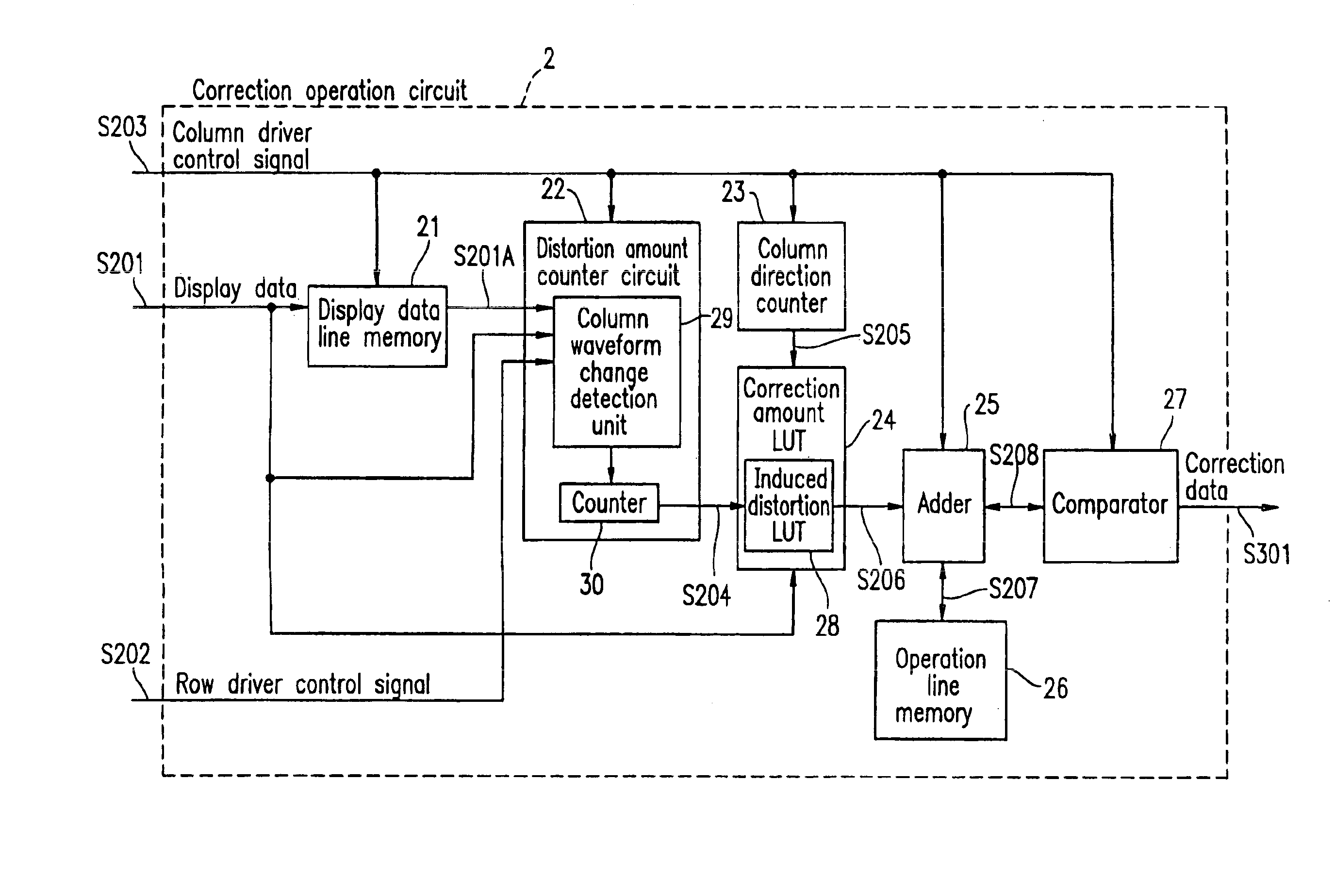
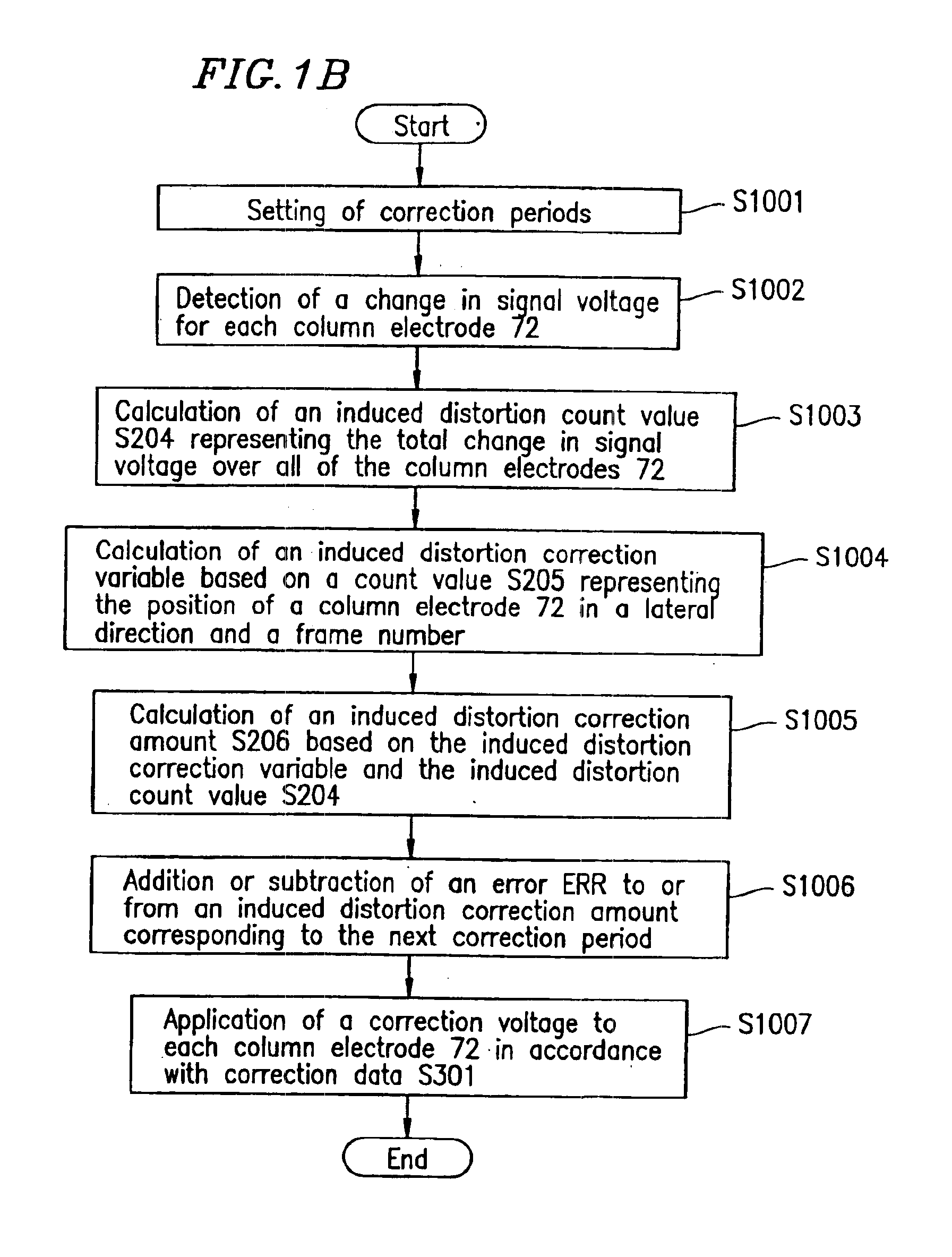
[0073]An LCD device and a driving method therefor according to Example 1 of the present invention will be described below, in which induced distortion crosstalk is optimally corrected.

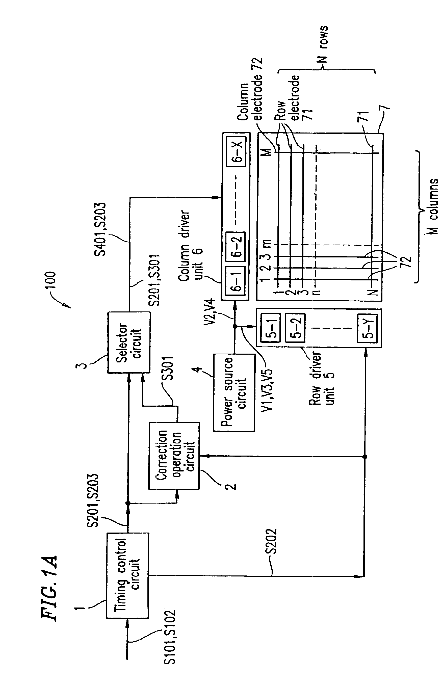
[0074]FIG. 1A is a schematic diagram showing an LCD device 100 according to Example 1 of the present invention. FIG. 1B is a flowchart showing an operation of the LCD device 100. The LCD device 100 includes a timing control circuit 1, a correction operation circuit 2, a selector circuit 3, a power source circuit 4, a row driver unit 5, a column driver unit 6, and a liquid crystal panel 7.

[0075]The timing control circuit 1 controls the timing of the entire system of the LCD device 100. The timing control circuit 1 receives a synchronization signal S102 and display data S101 and outputs a column driver control signal S203, display data S201, and a row driver control signal S202.

[0076]The timing control circuit 1 also generates a correction period required for performing correction processing described be...

example 2

[0118]Next, an LCD device and a driving method therefor according to Example 2 of the present invention will be described below. The LCD device of Example 2 has the same structure as that of Example 1 and further includes circuits which optimally correct blunt waveform crosstalk and the gradation phenomenon while correcting induced distortion crosstalk.

[0119]Blunt waveform crosstalk depends on at least either a change in signal voltage or a change in scanning voltage, but is independent of the position of each column electrode 72 in the lateral direction along the row electrodes 71 (FIG. 1A). The gradation phenomenon depends on the position of each column electrode 72 in the lateral direction, but is independent of a change in signal voltage.

[0120]In Example 1, the induced distortion crosstalk depends on at least either a change in signal voltage or a change in scanning voltage as well as the position of each column electrode 72 in the lateral direction. Therefore, the circuit for c...


PUM

PropertyMeasurementUnit
voltageaaaaaaaaaa
signal voltageaaaaaaaaaa
scanning voltageaaaaaaaaaa

Abstract

A method for driving a liquid crystal display device including a plurality of row electrodes intersecting a plurality of column electrodes, a scanning voltage applied to each of the row electrodes, and a signal voltage applied to each of the column electrodes, the method comprising the steps of: a) determining, for each of the column electrodes, correction data for correcting the signal voltage based on an increment or a decrement of an effective voltage value between each of row electrodes and each of the column electrodes; and b) applying a correction voltage for correcting the signal voltage to each of the column electrodes in accordance with the correction data. An increment or decrement of the effective voltage value may be due to i) at least either a blunt waveform or induced distortion of the signal voltage or ii) at least either a blunt waveform or induced distortion of the scanning voltage, or iii) both.

Description

BACKGROUND OF THE INVENTION[0001]1. Field of the Invention[0002]The present invention relates to a matrix type super twisted nematic (STN) liquid crystal display device and a method for driving the device. The device and method are used in office automation equipment such as a personal computer and word processor, multi-media personal digital assistants, audio and video equipment, game machines, and the like. More particularly, the present invention relates to a liquid crystal display device and a driving method therefor which can improve display quality.[0003]2. Description of the Related Art[0004]Conventional STN liquid crystal display (LCD) devices have a problem that as display capacity, such as liquid crystal capacity is increased, display irregularity depending on display patterns emerges, leading to a significant decrease in display quality. Such display irregularity is called crosstalk.[0005]An example of such crosstalk is one caused by induced distortion of scanning voltage...

Claims


Application Information

Patent Timeline
Patent Type & Authority Patents(United States)
IPC IPC(8): G09G3/36G02F1/133G09G3/20
CPCG09G3/3622G09G2320/0223G09G2320/0209
Inventor YASUNISHI, NORIOSATOH, FUTOSHI
Owner SHARP KK
Why Eureka
Try Eureka