Non volatile charge trapping dielectric memory cell structure with gate hole injection erase

a dielectric memory cell and non-volatile charge technology, applied in digital storage, semiconductor devices, instruments, etc., can solve the problems of bottom oxide damage and its interface with silicon substra

Active Publication Date: 2005-06-07
LONGITUDE FLASH MEMORY SOLUTIONS LTD
View PDF2 Cites 49 Cited by
  • Summary
  • Abstract
  • Description
  • Claims
  • Application Information

AI Technical Summary

Benefits of technology

[0011]A first aspect of the present invention is to provide a novel dielectric memory cell structure with band gap engineering to provide for gate hole injection erase techniques to be used for neutralizing a stored charge. The novel dielectric memory cell comprises a substrate, a multi-level charge trapping dielectric positioned on t

Problems solved by technology

A problem associated with hot hole injection is that it damages

Method used


Image

  • Non volatile charge trapping dielectric memory cell structure with gate hole injection erase
  • Non volatile charge trapping dielectric memory cell structure with gate hole injection erase
  • Non volatile charge trapping dielectric memory cell structure with gate hole injection erase

Examples


Embodiment Construction

[0032]The present invention will now be described in detail with reference to the drawings. In the drawings, like reference numerals are used to refer to like elements throughout.

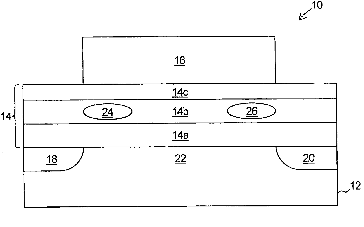
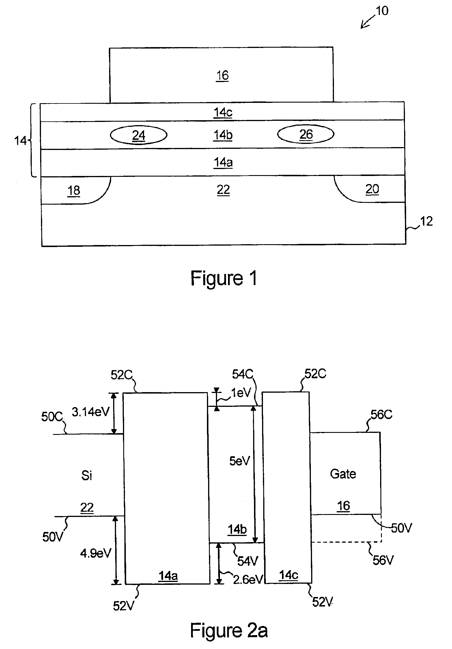
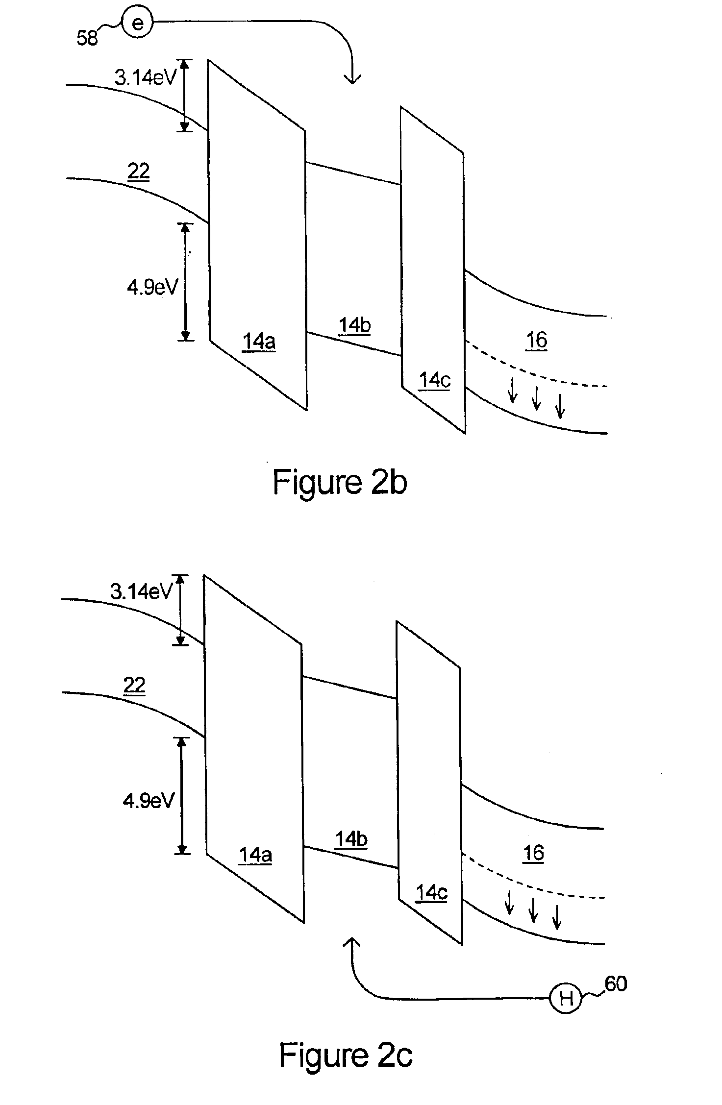
[0033]Referring to FIG. 1, a cross section view of a dielectric memory cell 10 formed on a semiconductor substrate 12 is shown. The diagram is not drawn to scale and the dimensions of some features are intentionally drawn larger than scale for purposes of showing clarity.

[0034]The memory cell 10 is shown as a substantially planar structure formed on the bulk substrate 12. However, it should be appreciated that the teachings of this invention may be applied to both planar, fin formed, and other dielectric memory cell structures which may be formed on either bulk substrates, SOI substrates or other substrate structures.

[0035]The memory cell 10 includes a multi layer charge trapping dielectric 14 positioned between the bulk substrate 12 and a control gate 16.

[0036]The bulk substrate 12 preferably comprises lig...


PUM


Abstract

A dielectric memory cell comprises a substrate which includes a source region, a drain region, and a channel region positioned there between. A multilevel charge trapping dielectric is positioned on the surface of the substrate and a control gate is positioned on the surface of the dielectric and is positioned over and aligned with the channel region. The multilevel charge trapping dielectric includes a tunneling dielectric layer, a charge trapping dielectric layer, and a top dielectric layer. The tunneling dielectric layer comprises a first dielectric material having a wide band gap between a tunneling dielectric layer valance band Fermi level and a tunneling dielectric layer conduction band Fermi level. The top dielectric layer comprises a second dielectric material having a valance band Fermi level approximately equal to the tunneling dielectric layer valance band Fermi level and having a conduction band Fermi level greater than the tunneling dielectric layer conduction band Fermi level. The charge trapping layer is positioned between the bottom layer and the top layer of a third dielectric with charge trapping properties.

Description

TECHNICAL FIELD[0001]The present invention relates generally to a non volatile charge trapping dielectric memory cell array and, more specifically to improvements in scalable non volatile dielectric memory cells and methods of erasing non volatile charge trapping dielectric memory cells.BACKGROUND OF THE INVENTION[0002]Conventional floating gate flash memory types of EEPROMs (electrically erasable programmable read only memory), utilize a memory cell characterized by a vertical stack of: i) a tunnel oxide (SiO2), ii) a polysilicon floating gate over the tunnel oxide, iii) an interlayer dielectric over the floating gate, and iv) a control gate over the interlayer dielectric. Such vertical stack is positioned over a crystalline silicon substrate. Within the substrate are a channel region positioned below the vertical stack and source and drain diffusions on opposing sides of the channel region.[0003]The floating gate flash memory cell is programmed by inducing hot electron injection f...

Claims


Application Information

Patent Timeline
IPC IPC(8): H01L21/02H01L21/28H01L29/423H01L29/66H01L29/792H01L29/40
CPCH01L21/28282H01L29/7923H01L29/42332H01L29/40117
Inventor KANG, JUN
Owner LONGITUDE FLASH MEMORY SOLUTIONS LTD
Why Eureka
Try Eureka