Magnetoresistive effect sensor with barrier layer smoothed by composition of lower shield layer

Inactive Publication Date: 2005-06-07
FUJIFILM HLDG CORP +1
View PDF9 Cites 16 Cited by
  • Summary
  • Abstract
  • Description
  • Claims
  • Application Information

AI Technical Summary

Benefits of technology

[0039]It is preferable that the magnetoresistive effect film pattern be formed so that the magnetoresistive effect element is formed on the lower shield so as to come into contact therewith via a base layer or directly, and in another form of the present invention, it is desirable that a conductor pattern be disposed below the base layer of the magnetoresistive effect film, the bottom part of the conductor pattern thereof being in contact with the lower shield.
[0040]Alternately, the lower conductor layer functions as a lower electrode that causes a sensing current to flow in the magnetoresistive effect film, the lower conductor layer being made of either an amorphous material or a microcrystalline material. It is desirable that the crystal grain diameter in the microcrystal forming the lower conductor layer be 5.4 nm or smaller. Additionally, the lower conductor layer is formed by sputtering.
[0041]As discussed above, when the surface roughness of the lower shield or t

Problems solved by technology

In either case, this leads to an increase in the barrier layer roughness.
Even in the case in which the roughness of the lower shield is small, however, if the roughness of the gap insulation layer or lower conductor layer formed thereover is great, this also results in an increase in the roughness of the barrier layer in the TMR film.
The problem that arises when the barrier layer roughness is large is that, in the TMR material the effective film thickness within the barrier layer becomes smaller.
Because the ferromagnetic coupling is a

Method used


Image

  • Magnetoresistive effect sensor with barrier layer smoothed by composition of lower shield layer
  • Magnetoresistive effect sensor with barrier layer smoothed by composition of lower shield layer
  • Magnetoresistive effect sensor with barrier layer smoothed by composition of lower shield layer

Examples


Example

[0059]Embodiments of a magnetoresistive effect sensor and a method for manufacturing a magnetoresistive effect sensor according to the present invention are described in detail below, with references made to relevant accompanying drawings.

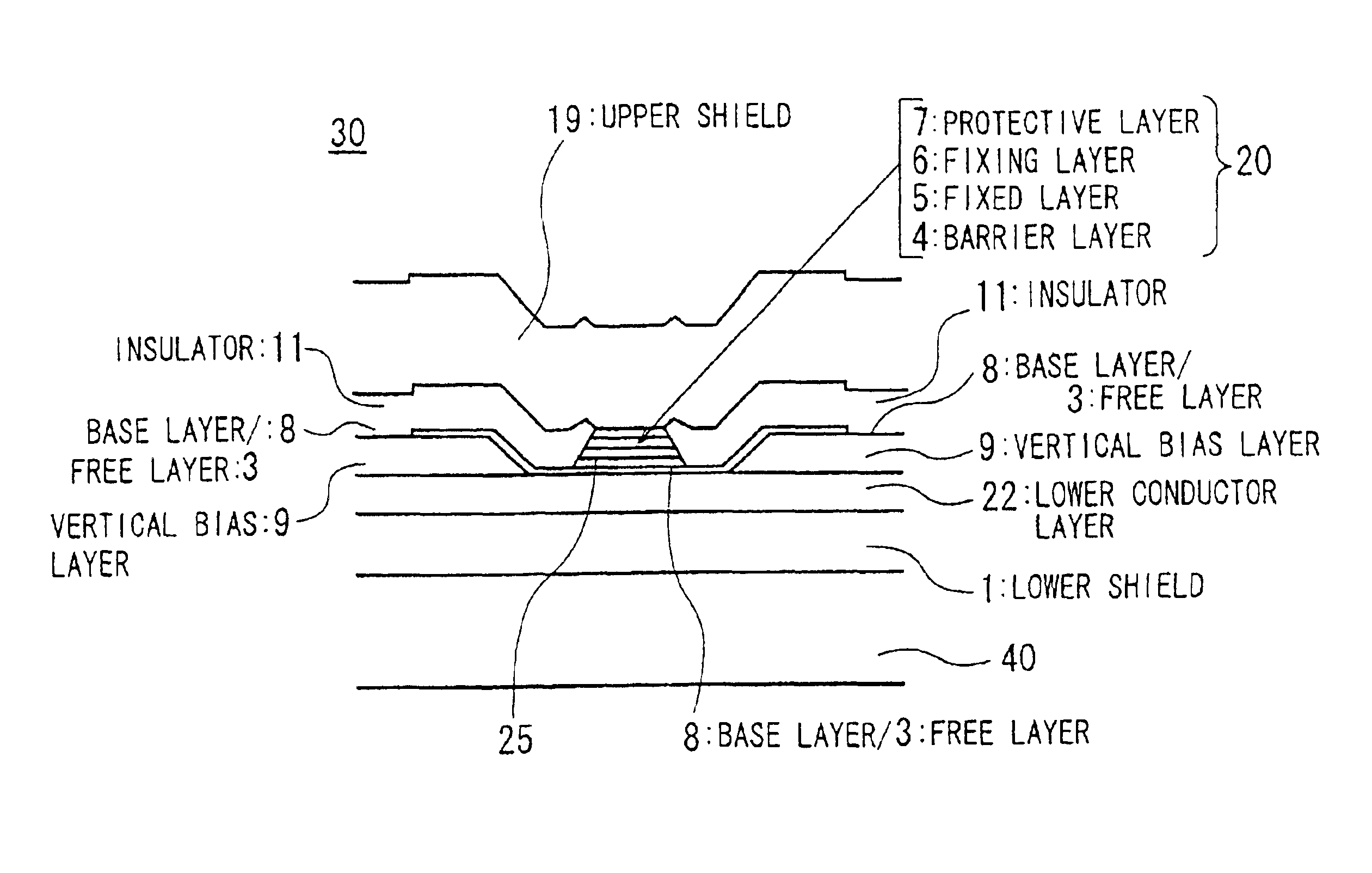
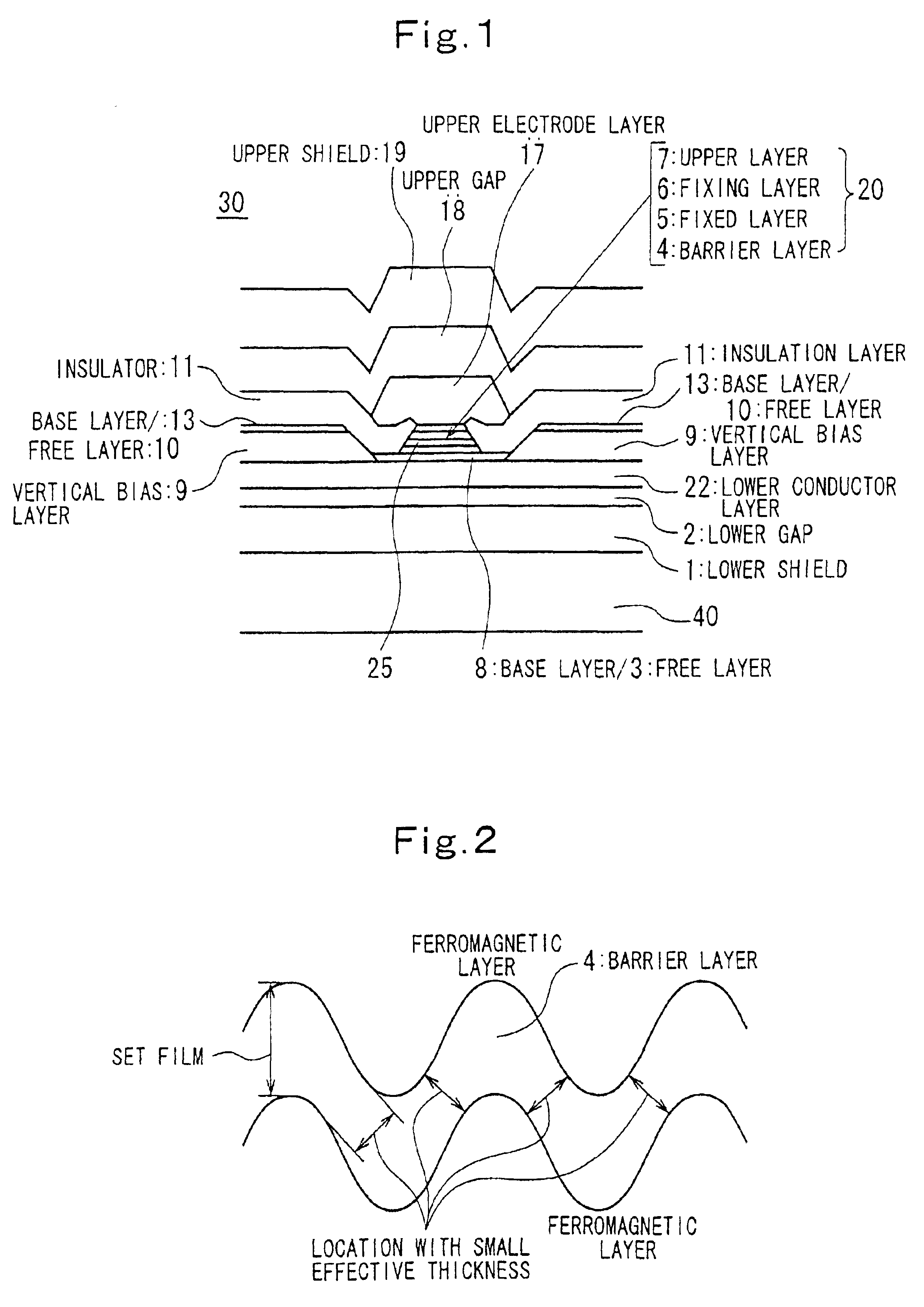
[0060]Specifically, FIG. 1 is a drawing showing the configuration of an embodiment of a magnetoresistive effect sensor according to the present invention, this drawing showing a magnetoresistive effect sensor 30 using a shielded-type magnetoresistive effect element 25 using a magnetoresistive effect film 20 with a basic configuration that is a combination of a free layer 3, a barrier layer 4 formed on the free layer 3, and a fixed layer 5 formed on the barrier layer 4, wherein a sensing current flows substantially perpendicularly to the magnetoresistive effect film, and wherein amorphous material or a microcrystalline material is used in a lower shield 1.

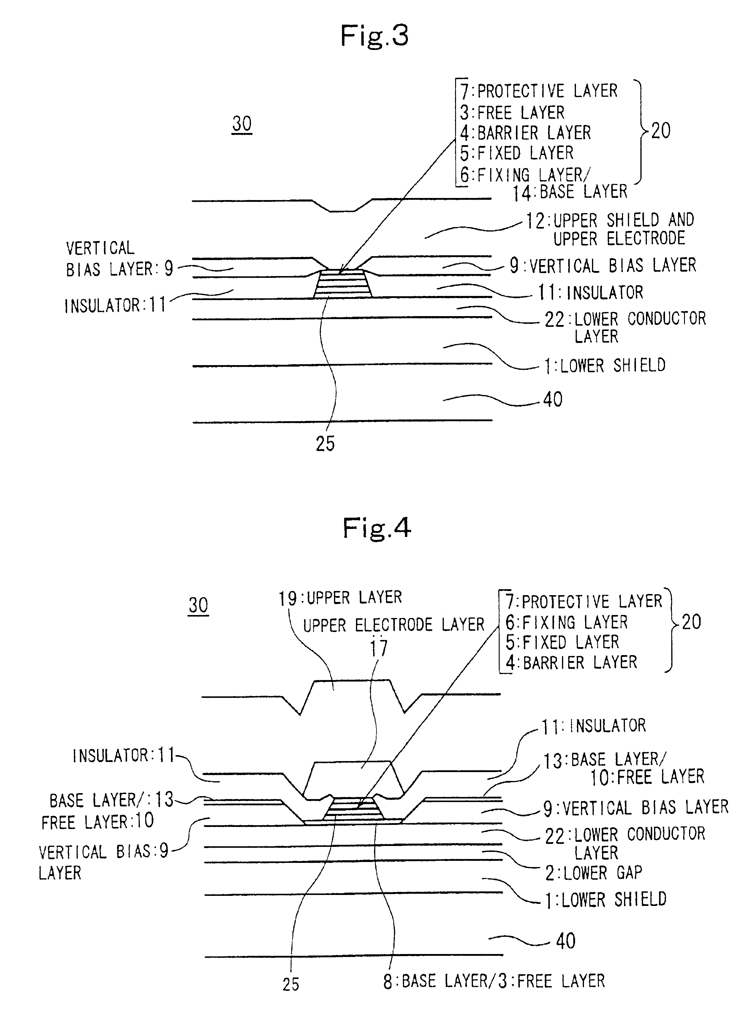
[0061]FIG. 3 shows the configuration of another embodiment of the present invention, this drawi...


PUM

PropertyMeasurementUnit
Nanoscale particle sizeaaaaaaaaaa
Lengthaaaaaaaaaa
Lengthaaaaaaaaaa

Abstract

A magnetoresistive effect sensor uses a shielded-type magnetoresistive effect element using a magnetoresistive effect film formed by a basic configuration of a combination of a free layer, a barrier layer formed on the free layer, and a fixed layer formed on the barrier layer, wherein a sensing current flows substantially perpendicular to the magnetoresistive effect film, and wherein an amorphous material or a microcrystalline material is used in a lower shield.

Description

BACKGROUND OF THE INVENTION[0001]1. Field of the Invention[0002]The present invention relates to a magnetic sensor for the purpose of reading an information signal recorded onto a magnetic medium.[0003]2. Related Art[0004]In the prior art, there has been disclosure of a magnetic reading transducer called a magnetoresistive (MR) sensor or head, and it is known that this is capable of reading data from a magnetic surface with a high linear density.[0005]An MR sensor detects a magnetic field signal by converting it to a change in resistance as a function of the strength and direction of magnetic flux sensed by a reading element. This MR sensor according to the prior art operates based on the anisotropic magnetoresistive (AMR) effect, whereby one component of the resistance of the reading element is proportional to cosine of the angle between the direction of magnetization and the direction of the detected current flowing in the element.[0006]A detailed description of the AMR effect is ...

Claims


Application Information

Patent Timeline
IPC IPC(8): G01R33/06G01R33/09G11B5/00G11B5/39G11B5/40G01R33/02G01R31/317H01F10/16H01F10/32H01L43/08H01L43/12
CPCB82Y10/00B82Y25/00G01R31/3171G01R33/093G11B5/3903G11B5/3909G11B5/00G11B2005/3996G11B5/40G11B5/39
Inventor HAYASHI, KAZUHIKOOHASHI, KEISHIISHIWATA, NOBUYUKINAKADA, MASAFUMIFUKAMI, EIZONAGAHARA, KIYOKAZUHONJO, HIROAKIFUJIKATA, JUNICHIISHIHARA, KUNIHIKOMORI, SHIGERU
Owner FUJIFILM HLDG CORP
Why Eureka
Try Eureka