Plane decoding method and device for three dimensional memories

a three-dimensional memory and plane decoding technology, applied in the field of memory devices, can solve the problems of reducing array efficiency, wasting chip area, and increasing the number of required contact holes

Active Publication Date: 2005-06-14
MACRONIX INT CO LTD
View PDF2 Cites 182 Cited by
  • Summary
  • Abstract
  • Description
  • Claims
  • Application Information

AI Technical Summary

Benefits of technology

[0005]Broadly speaking, the present invention enables a decoding scheme in which word line and bit line concepts are extended to planes a

Problems solved by technology

Thus, the multitude of contact holes requires a large area and leads to reduced array efficiency.
Thus, as the numb

Method used


Image

  • Plane decoding method and device for three dimensional memories
  • Plane decoding method and device for three dimensional memories
  • Plane decoding method and device for three dimensional memories

Examples


Embodiment Construction

[0021]Several exemplary embodiments of the invention will now be described in detail with reference to the accompanying drawings.

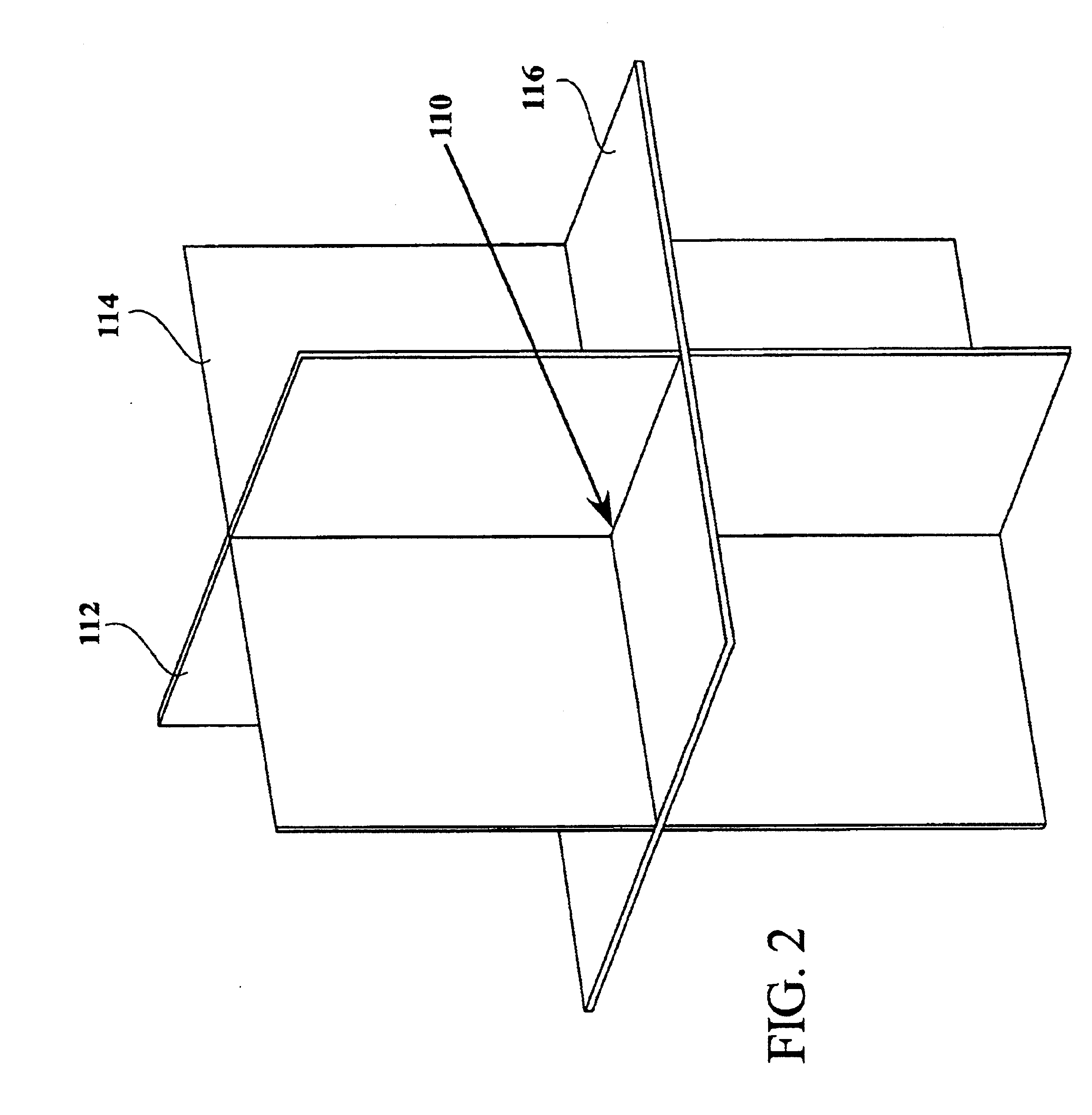
[0022]In accordance with the present invention, a multi-layer memory structure, i.e., a memory structure having multiple levels of memory core cells, that incorporates a plane decoding scheme in place of a line decoding scheme is provided. A memory core cell of the multi-layer structure is accessed by intersection of three planes. Two of the three planes access an active terminal of memory core devices, where the memory core devices are defined in each level of the multi-layer structure. One of the three planes accesses an active terminal of the memory core devices, where the memory core devices are defined within a single level of the multi-layer structure. Thus, as two of the three planes include word lines or bit lines that are electrically connected within the corresponding plane, via holes for the contacts may be directly stacked upon each other. Thus...


PUM


Abstract

A multi-layer memory device is provided. The multi-layer memory device includes multiple layers of memory core cells. A word plane electrically connecting each first active terminal of the multiple layers of the memory core cells intersected by the word plane is included. A drain plane substantially orthogonal to the word plane is provided. The drain plane electrically connects each second active terminal of the multiple layers of the memory core cells intersected by the drain plane. A source plane substantially orthogonal to both the word plane and the drain plane is included. The source plane electrically connects each third active terminal of the memory core cells within a single level. In one embodiment, the memory core cells are defined by a device having three active terminals.

Description

BACKGROUND OF THE INVENTION[0001]The present invention relates generally to memory devices and, more particularly, to a three dimensional memory cell structure utilizing a plane decoding technique.[0002]Conventional memory architectures employ word lines and bit lines to access the memory cells defined by the memory architecture. Three dimensional memory structures include several memory layers that are stacked upon each other. FIG. 1 illustrates the large area for contact holes required for the independent word lines and bit lines for a three dimensional memory structure. Peripheral circuits 104 are connected to the word lines and bit lines from layers 100a-100n through corresponding contact holes 102a-102n. For example, lines 100a-100n may represent bit lines from the first, second, third and nth layer of the memory structure, respectively. Since lines 100a-100n of the different layers are independent, then respective contact holes 102a-102n cannot be common. It should be apprecia...

Claims


Application Information

Patent Timeline
IPC IPC(8): G11C5/06G11C11/34H01L21/70H01L21/82H01L27/10G11C5/02H01L21/822H01L21/8246H01L27/06H01L27/112
CPCG11C5/025G11C5/06H01L27/1122H01L27/0688H01L27/112H01L21/8221H10B20/30H10B20/00
Inventor LUE, HANG-TING
Owner MACRONIX INT CO LTD
Why Eureka
Try Eureka