Optoelectronic assembly with embedded optical and electrical components

Inactive Publication Date: 2005-06-14
LERNER STEVE +1
View PDF22 Cites 1 Cited by
  • Summary
  • Abstract
  • Description
  • Claims
  • Application Information

AI Technical Summary

Benefits of technology

[0019]In general, in another aspect, the invention features a method of coupling an optical conductor to a light emitting surface of an optoelectronic semiconductor device. The method includes the following steps. First, providing a multilayer substrate having first and second sets of patterned layers. The first set of patterned layers includes at least one metal layer and at least one dielectric layer and the second set of patterned layers includes at least one polymeric layer. Next, forming a cavity within the at least one polymeric layer. The cavity is adapted to receive and electrically connect the optoelectronic semiconductor device to the metal layer. Next, forming a groove within the polymeric layer. The groove leads to the cavity and is adapted to receive and optically connect the optical conductor to the light emitting surface of the optoelectronic semiconductor device. Finally, precisely positioning the optoelectronic semiconductor device and the optical conductor within the cavity and the groove, respectively, so that light emitted from the light emitting surface of the optoelectronic semiconductor device couples to an optical surface of the optical conductor.
[0020]Implementations of this aspect of the invention may include one or more of the following features. The method may further include forming a first opening in a cavity wall and positioning the optoelectronic semiconductor device within the cavity so that light emitted from the light emitting surface exits the cavity via the first opening. The method may further include forming a second opening in a groove wall, wherein the second opening is aligned with the first opening, thereby allowing light exiting the cavity through the first

Problems solved by technology

This is an expensive method, which is not compatible with standard microelectronic infrastructures and processes.
These positioning elements also increase the complexity and cost of the method.
This technique involves a great number of processing steps and is limited to substrates that a

Method used


Image

  • Optoelectronic assembly with embedded optical and electrical components
  • Optoelectronic assembly with embedded optical and electrical components
  • Optoelectronic assembly with embedded optical and electrical components

Examples


Example

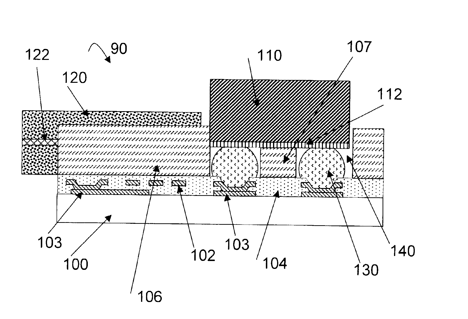
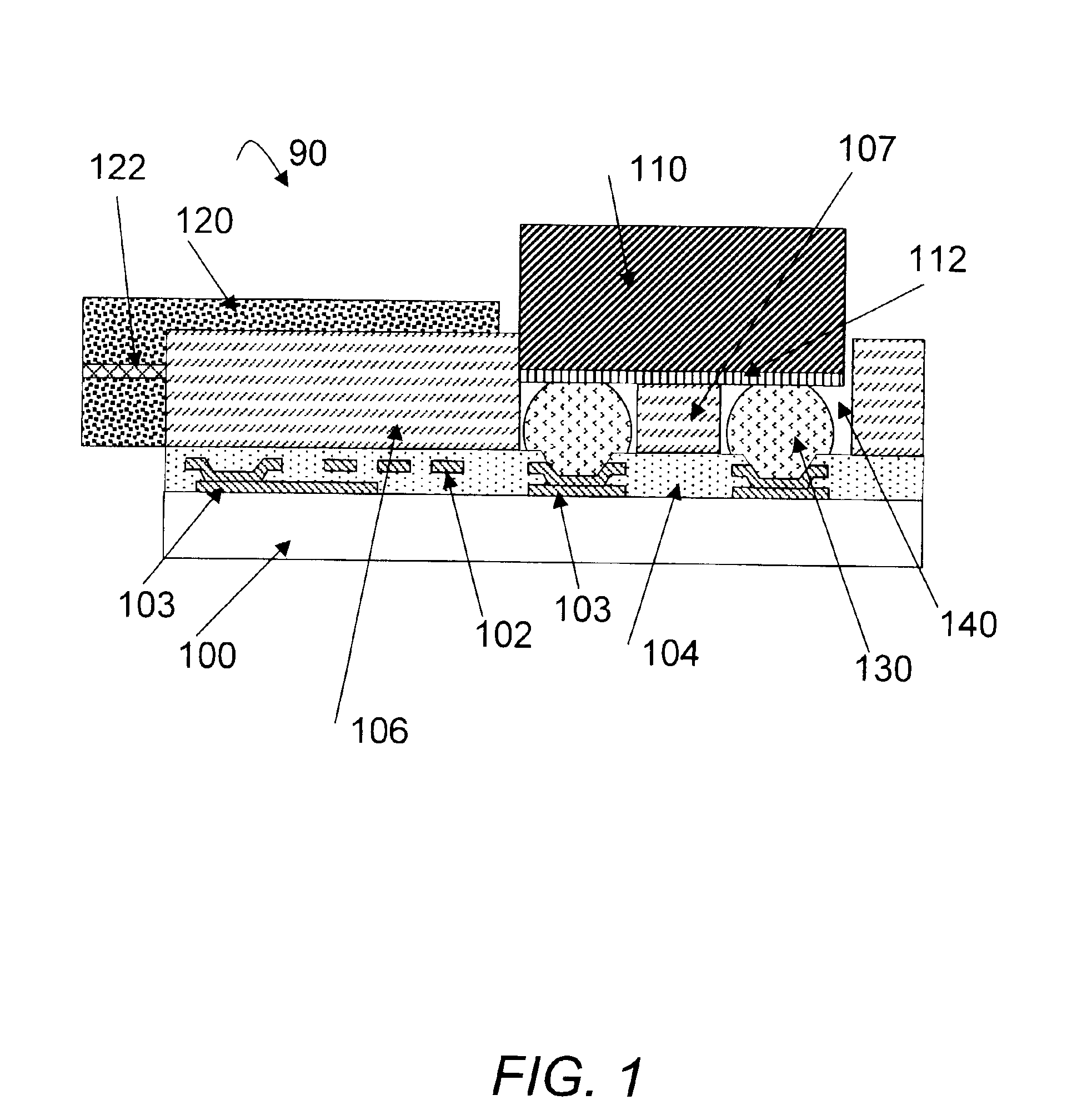
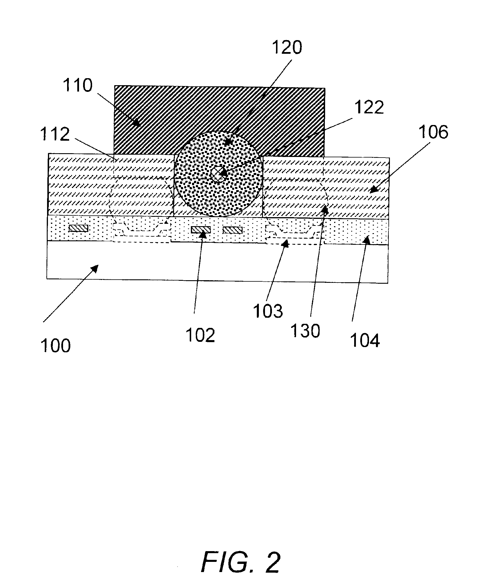
[0028]Referring to FIG. 1, the optoelectronic assembly 90 includes a carrier substrate 100, a dielectric layer 104 with embedded patterned metal layers 102, 103, and a polymeric layer 106. Dielectric layer 104 is positioned on top of the carrier substrate 100 and the polymeric layer 106 is positioned on top of the dielectric layer 104. The thickness of the carrier substrate 100 and the dielectric layer 104 is in the range of 10 to 20 micrometers. The thickness of the polymeric layer 106 varies between 30 and 150 micrometers. The assembly 90 further includes a semiconductor die 110, connected to the patterned metal layers 103 via metal bonding pads 130. In a preferred embodiment the semiconductor die 110 is flipchip mounted into a cavity 140 formed within the polymeric layer 106. The semiconductor die 110 may be an edge emitting laser, photodiode or other semiconductor optical devices. The polymeric layer is patterned to include a groove 150, stoppers 108 (shown in FIG. 3), cavity 14...


PUM


Abstract

The invention provides an optoelectronic assembly for coupling an optical conductor to a light emitting surface of an optoelectronic semiconductor device on a substrate. The optoelectronic assembly includes a multilayer having a cavity adapted to receive and electrically connect the optoelectronic semiconductor device to the multilayer substrate and a groove leading to the cavity and being adapted to receive and optically connect the optical conductor to the light emitting surface of said optoelectronic semiconductor device. The optoelectronic semiconductor device and the optical conductor are precisely positioned within the cavity and the groove, respectively, so that light emitted from the light emitting surface of the optoelectronic semiconductor device couples to an optical surface of the optical conductor.

Description

CROSS REFERENCE TO RELATED CO-PENDING APPLICATIONS[0001]This application claims the benefit of U.S. provisional application Ser. No. 60 / 388,437 filed on Jun. 13, 2002 and entitled INTEGRATED OPTOELECTRONIC ASSEMBLY WITH EMBEDDED OPTICAL AND ELECTRICAL COMPONENTS which is commonly assigned and the contents of which are expressly incorporated herein by reference.FIELD OF THE INVENTION[0002]The invention relates to an optoelectronic assembly, and more particularly, to an optoelectronic assembly with embedded optical and electrical components on a substrate.BACKGROUND OF THE INVENTION[0003]There are many methods for manufacturing optoelectronic assemblies that include integrated optical and electrical devices and components on a substrate. The optical and electrical devices and components may be among others optical fibers, lenses, mirrors, light emitting diodes, laser diodes, photodiodes, detectors, semiconductor devices, capacitors, inductors and resistors.[0004]Several prior art meth...

Claims


Application Information

Patent Timeline
IPC IPC(8): G02B6/42
CPCG02B6/4214G02B6/423G02B6/4231H01L2224/16225
Inventor LERNER, STEVETRUZZI, CLAUDIO
Owner LERNER STEVE
Why Eureka
Try Eureka