Lateral double-diffused MOS transistor having multiple current paths for high breakdown voltage and low on-resistance

Active Publication Date: 2005-06-21
SEMICON COMPONENTS IND LLC
View PDF2 Cites 75 Cited by
  • Summary
  • Abstract
  • Description
  • Claims
  • Application Information

AI Technical Summary

Benefits of technology

[0011]The present invention provides a lateral double-diffused MOS transistor having

Problems solved by technology

However, it is also well-known that low on-resistance and high breakdown volta

Method used


Image

  • Lateral double-diffused MOS transistor having multiple current paths for high breakdown voltage and low on-resistance
  • Lateral double-diffused MOS transistor having multiple current paths for high breakdown voltage and low on-resistance
  • Lateral double-diffused MOS transistor having multiple current paths for high breakdown voltage and low on-resistance

Examples


Example

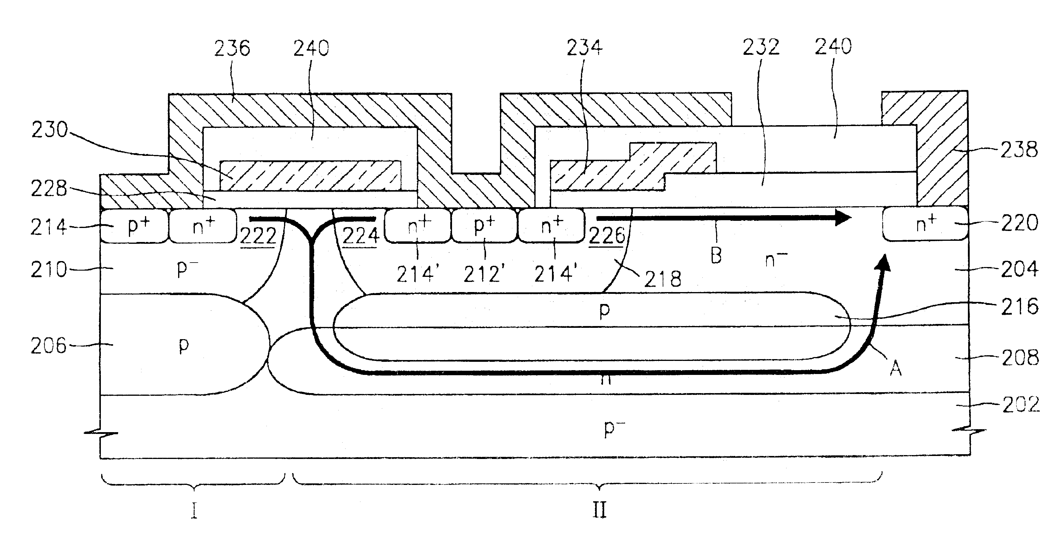
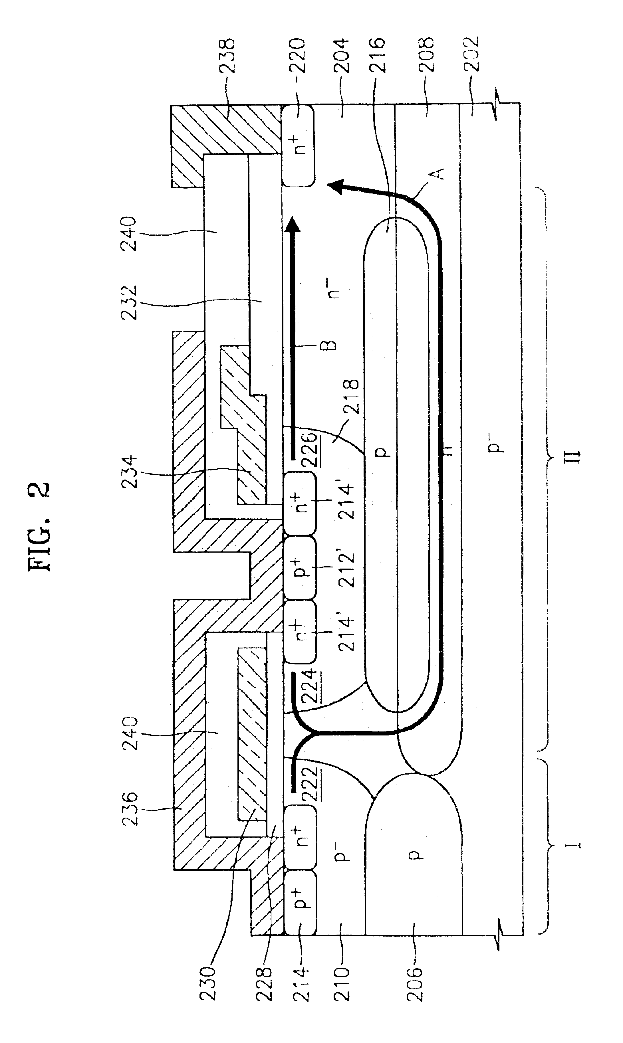
[0036]Hereinafter, embodiments of the present invention will be described in detail with reference to the accompanying drawings. This invention may, however, be embodied in many different forms and should not be construed as being limited to the embodiments set forth herein.

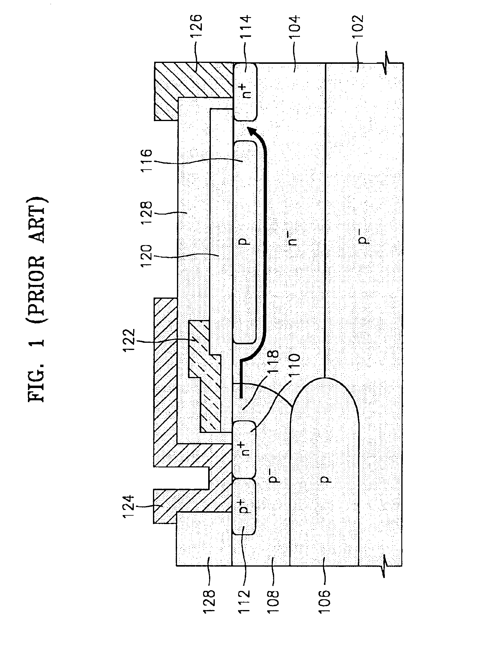
[0037]FIG. 2 is a cross-sectional view illustrating a structure of a lateral double-diffused MOS (LDMOS) transistor having double current paths according to an embodiment of the present invention. Referring to FIG. 2, an n−-type epitaxial layer 204 is arranged on a p−-type semiconductor substrate 202. The n−-type epitaxial layer 204 is used as a drift region. A first p-type buried layer 206 and a second n-type buried layer 208 are formed at the boundary between the p−-type semiconductor substrate 202 and the n−-type epitaxial layer 204, respectively. The first p-type buried layer 206 is arranged in a first portion I, and the second n-type buried layer 208 is arranged in a second portion II. A third p-type buried ...


PUM


Abstract

A lateral double-diffused MOS (LDMOS) transistor is provided. The LDMOS transistor includes a semiconductor substrate 202 formed of a material having p-conductivity type impurities, a drift region formed of a material having n-conductivity type impurities on the semiconductor substrate, a first buried layer 206 of p-type material and a second buried layer 208 formed of n-type material. Layers 206 and 208 are arranged at the boundary between the semiconductor substrate and the drift region. A first well region 210 of p-type material contacts the first buried layer 206 n-type in a first portion 1 of the drift region. A first source region 214 conductivity in a predetermined upper region of the first well region, a drain region formed of a material having second conductivity type impurities in a predetermined region of the drift region, the drain region being spaced a predetermined gap apart from the first well region, a third buried layer formed of a material having first conductivity type impurities in a second region of the drift region, the third buried layer being overlapped with a part of an upper portion of the first buried layer, a second well region formed of a material having first conductivity type impurities in the second region of the drift region, the second well region being overlapped with the third buried layer, a second source region formed of a material having second conductivity type impurities in a predetermined upper region of the second well region, a gate insulating layer formed in a first channel region inside the first well region and in a second channel region inside the second well region, a gate electrode formed on the gate insulating layer, a source electrode formed to be electrically connected to the first source region and the second source region, and a drain electrode formed to be electrically connected to the drain region.

Description

BACKGROUND OF THE INVENTION[0001]This application claims the priority of Korean Patent Application No. 2003-22210, filed on Apr. 9, 2003, in the Korean Intellectual Property Office, the disclosure of which is incorporated herein in its entirety by reference.[0002]1. Field of the Invention[0003]The present invention relates to a lateral double-diffused MOS transistor, and more particularly, to a lateral double-diffused MOS transistor having multiple current paths for a high breakdown voltage and a low on-resistance.[0004]2. Description of the Related Art[0005]In general, high-voltage integrated circuits (ICs) in which at least one high-voltage transistor is arranged on the same chip together with low-voltage circuits are widely used in a variety of electrical applications. In these ICs, a lateral double-diffused MOS (LDMOS) transistor is an important high-voltage device. It is well-known to design LDMOS transistorsby, minimizing on-resistance while maintaining a high breakdown voltag...

Claims


Application Information

Patent Timeline
IPC IPC(8): H01L29/76H01L29/66H01L31/101H01L31/113H01L29/06H01L29/08H01L29/10H01L29/78
CPCH01L29/0634H01L29/0878H01L29/7816H01L29/7809H01L29/1095H01L29/78
Inventor JEON, CHANG-KIKIM, JONG-JIBCHOI, YOUNG-SUK
Owner SEMICON COMPONENTS IND LLC
Why Eureka
Try Eureka