

Semiconductor device and method of manufacturing the same
- Summary
- Abstract
- Description
- Claims
- Application Information
AI Technical Summary
Benefits of technology
Problems solved by technology
Method used
Image

Examples
Embodiment Construction
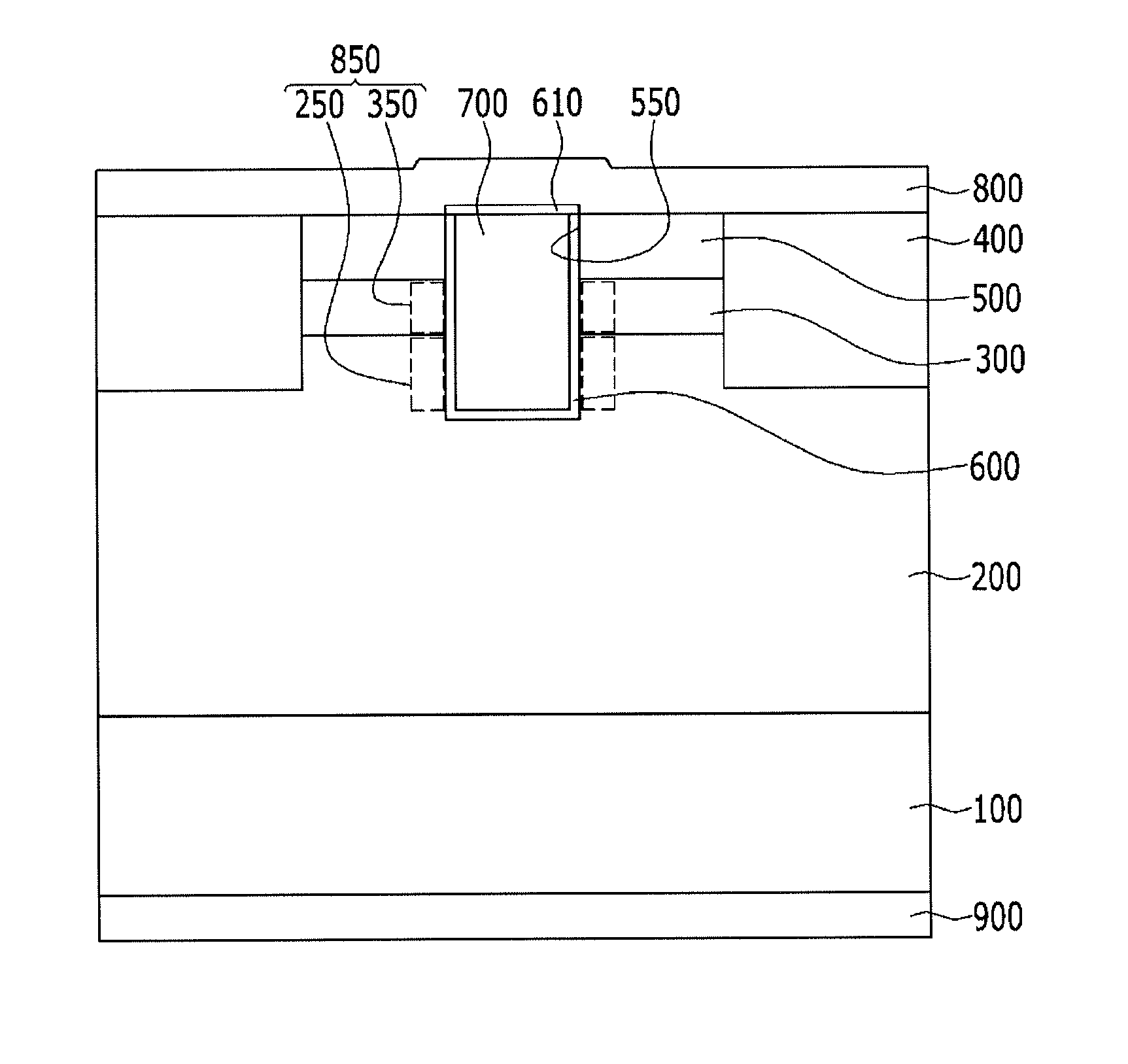
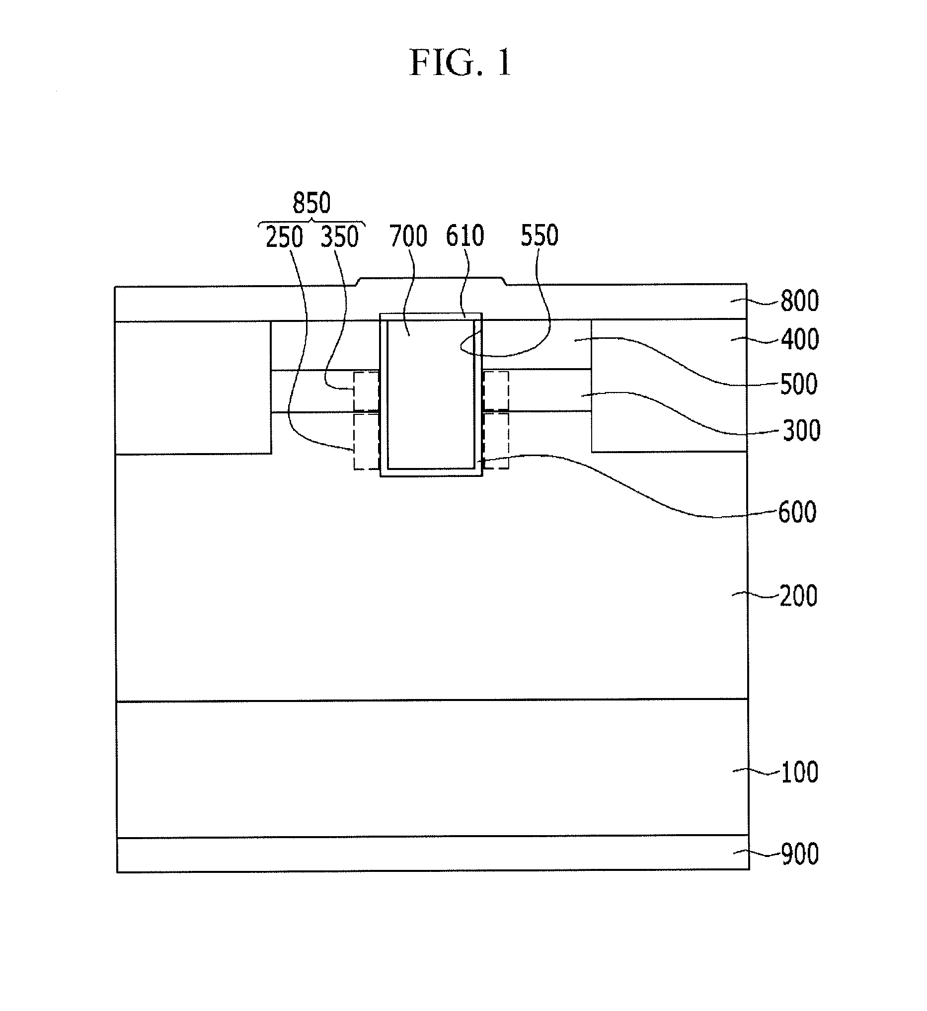
[0019]Reference will now be made in detail to various embodiments of the present invention(s), examples of which are illustrated in the accompanying drawings and described below. While the invention(s) will be described in conjunction with exemplary embodiments, it will be understood that present description is not intended to limit the invention(s) to those exemplary embodiments. On the contrary, the invention(s) is / are intended to cover not only the exemplary embodiments, but also various alternatives, modifications, equivalents and other embodiments, which may be included within the spirit and scope of the invention as defined by the appended claims.
[0020]In the drawings, the thickness of layers, films, panels, regions, etc., are exaggerated for clarity. It will be understood that when a layer is referred to as being “on” another layer or substrate, it can be directly on the other layer or substrate, or intervening them may also be present.
[0021]FIG. 1 is a cross-sectional view o...
PUM
 Abstract
Description
Claims
Application Information