Power mos transistor and manufacturing method therefor

Active Publication Date: 2016-09-22
SUZHOU ORIENTAL SEMICONDUCTOR CO LTD
View PDF1 Cites 11 Cited by
  • Summary
  • Abstract
  • Description
  • Claims
  • Application Information

AI Technical Summary

Benefits of technology

[0024]Compared with the prior art, the present invention has the following remarkable advantages:
[0025]Firstly, in the power MOS transistor of the present invention, the second U-shaped trench is provided below the first U-shaped trench, which enables the field oxidation stress transition region to be extended, so as to well solve the problem of current leakage caused by the field oxide stress and improve the reliability of the device.
[0026]Secondly, the charge compensation region can be formed in the drift region below the second U-shaped trench of the power MOS transistor, thus fo

Problems solved by technology

However, the power MOS transistor of the U-shaped trench needs to be provided with a deep trench, so that the manufacturing process of the gate oxide layer is very complicated, the manufacturing cost is high, and the yield of the device is reduced.
However, the power MOS transistor also has obvious shortcomings as below: 1. the transition region between the thick field oxide layer at the bottom of the U-shaped trench and the thin gate o

Method used


Image

  • Power mos transistor and manufacturing method therefor
  • Power mos transistor and manufacturing method therefor
  • Power mos transistor and manufacturing method therefor

Examples


Example

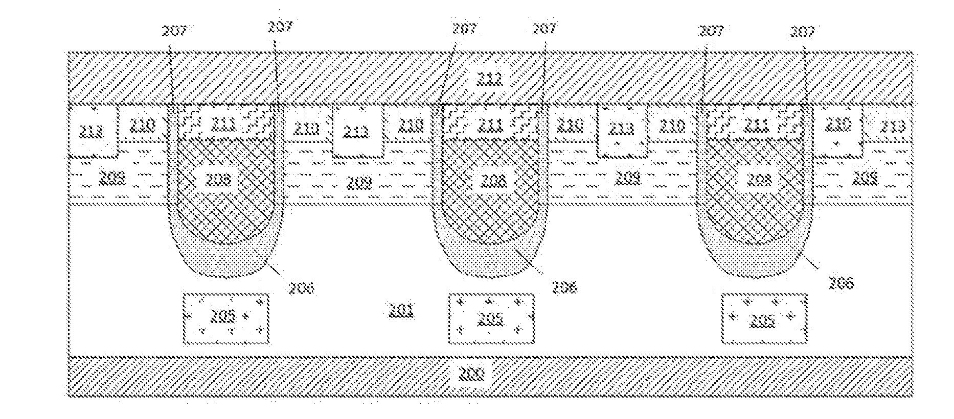
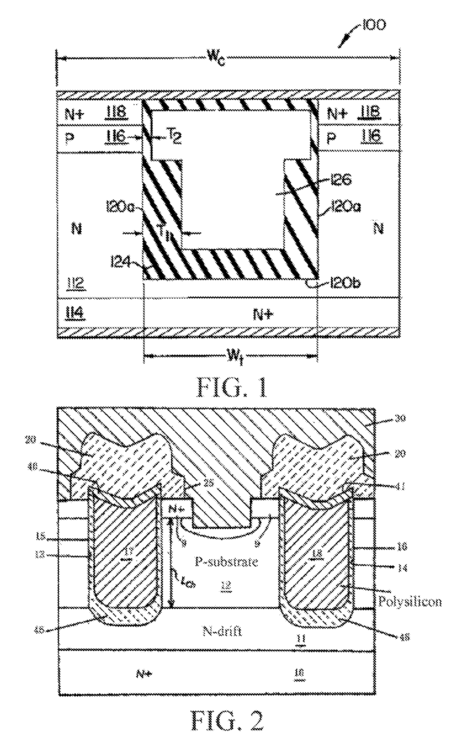
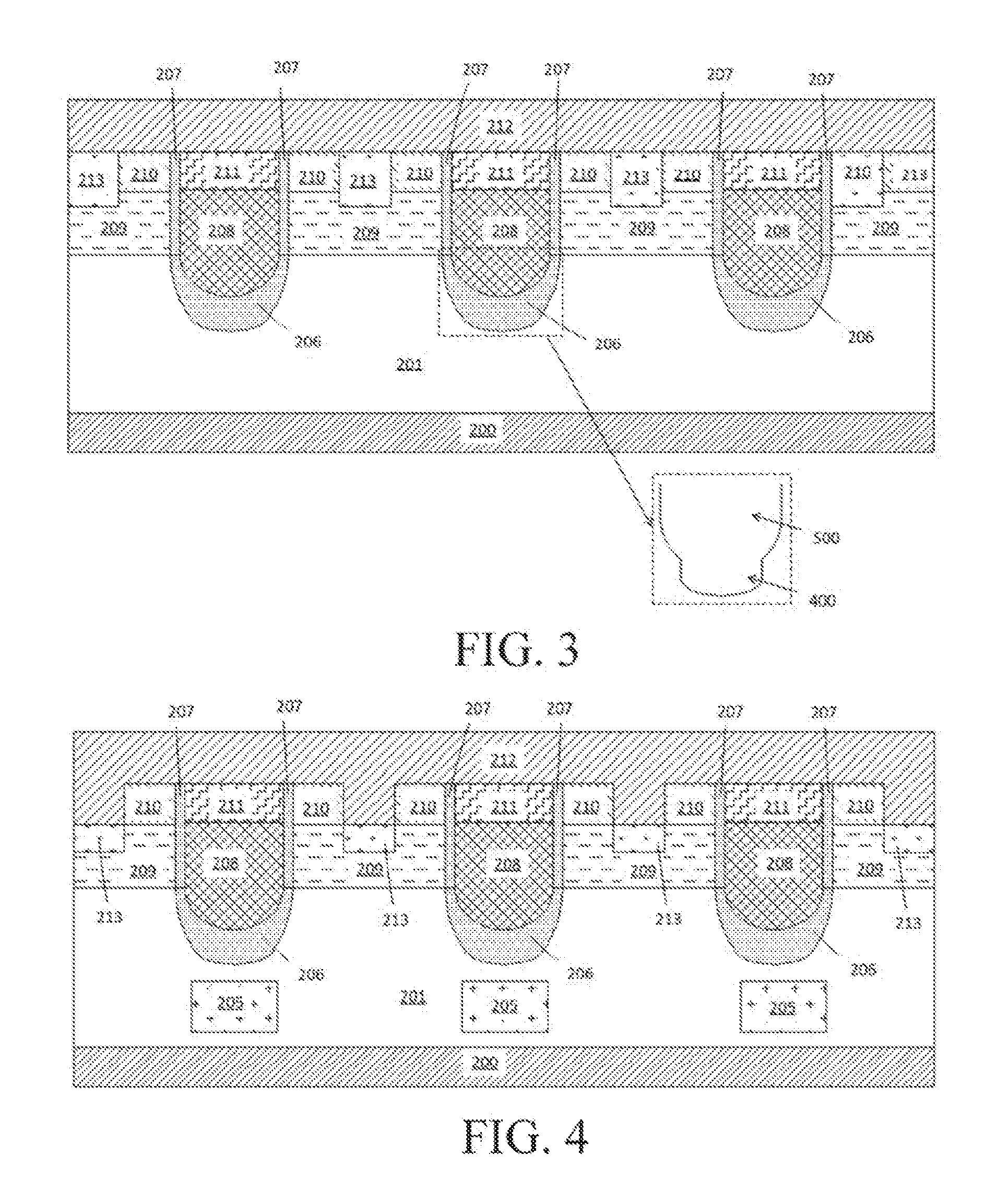
[0037]For clearly illustrating the embodiments of the present invention, the figures listed in the drawings of the description magnify the thicknesses of the layers and the regions of the present invention, and the sizes of the shown figures do not represent the actual sizes; the drawings are schematic, and should not limit the scope of the present invention. The embodiments listed in the description should not be merely limited to the specific shapes of the regions shown in the drawings, but comprise the obtained shapes such as deviation caused by manufacturing, as well as the obtained curves are usually bent or round, which are all represented with a rectangle in the embodiments of the present invention; meanwhile, in the following description, the used term “semiconductor substrate” can be regarded as including a semiconductor wafer being processed as well as other film layers manufactured thereon, such as an epitaxial layer formed on the semiconductor substrate.

[0038]The followi...


PUM


Abstract

The present invention discloses a power Metal Oxide Semiconductor (MOS) transistor, wherein a second U-shaped trench is formed below a first U-shaped trench, so that a field oxidation stress transition region can be extended, so a s to greatly reduce current leakage caused by the field oxidation stress and improve the reliability of the device; and a charge compensation region is provided in a drift region at the bottom of the second U-shaped trench, and a super-junction structure is formed between the charge compensation region and the drift region to improve the breakdown voltage of the power device. According to the present invention, the second U-shaped trench and the charge compensation region are formed by a self-aligning process, so that the technical process is simple, reliable and easy to control, and can reduce the manufacturing cost of the power MOS transistor and improve its yield.

Description

FIELD OF THE INVENTION[0001]The present invention relates to the technical field of semiconductor power devices, and more particularly to a power MOS transistor and a manufacturing method thereof.DESCRIPTION OF RELATED ART[0002]With continuous deep development of modern microelectronic technology, the power MOS transistor gradually replaces bipolar devices and becomes the mainstream of the development of semiconductor power devices nowadays due to its advantages such as high input impedance, low loss, high switching speed, no secondary breakdown, wide safe operating area, good dynamic performance, easiness in being coupled with the anterior pole to realize high current, as well as high conversion efficiency. Conventional. semiconductor power devices mainly comprise the types such as planar diffusion type MOS transistors and trench type MOS transistors. Taking the trench type MOS transistor as an example, the area of the device adopting the vertical channel structure is much smaller ...

Claims


Application Information

Patent Timeline
IPC IPC(8): H01L29/66H01L29/78H01L29/423H01L21/28H01L21/265H01L21/306H01L21/02H01L29/10H01L29/15
CPCH01L29/66734H01L29/1095H01L29/7813H01L29/42368H01L21/28035H01L21/26506H01L21/306H01L21/02238H01L29/157H01L21/3083H01L21/32H01L29/41766H01L29/7397H01L29/0623H01L29/0634H01L29/0696H01L29/66348H01L29/7396H01L29/78
Inventor LIU, WEILIU, LEILIN, XIWANG, PENGFEIGONG, YI
Owner SUZHOU ORIENTAL SEMICONDUCTOR CO LTD
Why Eureka
Try Eureka