Semiconductor device and method of manufacturing the same

Inactive Publication Date: 2005-05-24
SEMICON COMPONENTS IND LLC
View PDF11 Cites 52 Cited by
  • Summary
  • Abstract
  • Description
  • Claims
  • Application Information

AI Technical Summary

Benefits of technology

[0015]Therefore, a second object of the present invention is to provide a semiconductor device which is responsible to requests for the higher breakdown voltage and the reduction in its ON-resistance and also enables the higher integration density, and a method of manufacturing the same.
[0016]Therefore, a third object of the present inventio

Problems solved by technology

However, in the CMOS structure in the prior art the process for manu

Method used


Image

  • Semiconductor device and method of manufacturing the same
  • Semiconductor device and method of manufacturing the same
  • Semiconductor device and method of manufacturing the same

Examples


first embodiment

[0047]A semiconductor device and a method of manufacturing the same according to the present invention will be explained with reference to the accompanying drawings hereinafter.

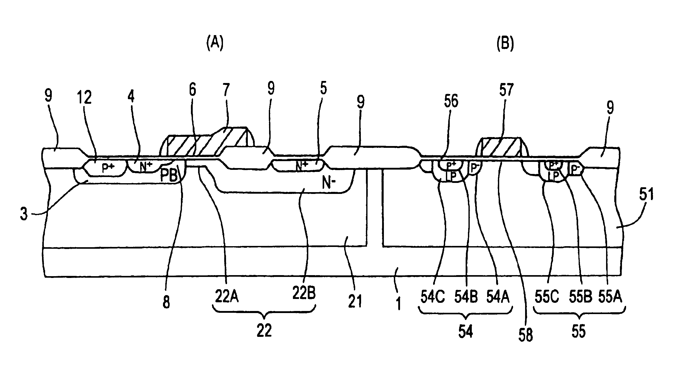
[0048]FIG. 1 is a sectional view showing the semiconductor device and the method of manufacturing the same according to the first embodiment of the present invention. A configuration consisting of the N-channel LDMOS transistor (A) and the P-channel high breakdown voltage MOS transistor (B) is shown as an example. In this case, same symbols are affixed to constituent elements similar to those in the prior art, and their explanation will be simplified.

[0049]In FIG. 1, 1 denotes one conductivity type, e.g., P-type semiconductor substrate, and 21 denotes a P-type well region. An N−-type layer 22 as well as the P-type body region (PB) 3 is formed in the P-type well region 21. The N-type diffusion region 4 is formed in the P-type body region 3, and the N-type diffusion region 5 is also formed in the N−-type layer ...

third embodiment

[0073]Next, the present invention will be explained hereunder.

[0074]FIG. 8 is a sectional view showing an LDMOS transistor according to the third embodiment. The N-channel LDMOS transistor structure is shown as an example. Although the explanation of the P-channel LDMOS transistor structure is omitted, it is well known that such structure has the similar structure except for the different conductivity type. In this case, same symbols are affixed to constituent elements similar to those in the prior art, and their explanation will be simplified.

[0075]In FIG. 8, 1 denotes a conductivity type, e.g., P-type semiconductor substrate, and 21 denotes the P-type well region. The N−-type layer 22 as well as the P-type body region 3 is formed in the P-type well region 21. The N-type diffusion region 4 is formed in the P-type body region 3, and the N-type diffusion region 5 is formed in the N−-type layer 22. The gate electrode 7 is formed on the surface of the substrate via the gate insulating ...


PUM


Abstract

In order to improve the characteristics of the high breakdown voltage MOS, a semiconductor device of the present invention is characterized in that an LDMOS transistor, which comprises a source region 4, a channel region 8, and a drain region 5, and a gate electrode 7 formed on the channel region 8, and a drift region formed between the channel region 8 and the drain region 5, wherein an N-type low concentration layer 22 serving as the drift region is formed shallowly at least below the gate electrode 7 (first N-type layer 22A) but formed deeply in a neighborhood of the drain region 5 (second N-type layer 22B).

Description

BACKGROUND OF THE ART[0001]1. Technical Field[0002]The present invention relates to a semiconductor device and a method of manufacturing the same and, more particularly, a technology for an LD (Lateral Double Diffused) MOS transistor as a high voltage element employed in a liquid crystal driving IC, etc., for example.[0003]2. Related Art of the Invention[0004]In the LDMOS transistor structure, a new diffusion region is formed by diffusing a different conductivity type impurity into a diffusion region formed on the surface side of a semiconductor substrate, and then a difference in lateral diffusion lengths of these diffusion regions is utilized as an effective channel length. Thus, since a short channel can be formed, the LDMOS transistor is suitable for the low ON-resistance device.[0005]FIG. 18 is a sectional view showing the LDMOS transistor in the prior art. The N-channel LDMOS transistor structure is shown as an example. In this case, although explanation of the P-channel LDMOS...

Claims


Application Information

Patent Timeline
IPC IPC(8): H01L29/76H01L27/148H01L29/68H01L29/66H01L29/94H01L31/062H01L31/06H01L21/336H01L21/8234H01L29/08H01L29/78
CPCH01L21/823418H01L27/1463H01L29/7835H01L29/66659H01L29/7833H01L21/823462H01L29/0847
Inventor KIKUCHI, SHUICHIAKAISHI, YUMIKO
Owner SEMICON COMPONENTS IND LLC
Why Eureka
Try Eureka