This helps you quickly interpret patents by identifying the three key elements:
Problems solved by technology
Method used
Benefits of technology
Benefits of technology
This patent is about a new configuration for a semiconductor device that separates different regions that require tolerance and ON-resistance. This separation helps to minimize loss of area and makes it easier to dispose of the device. The ratio of two different semiconductor regions in the device affects its tolerance and ON-resistance. By adjusting the ratio for each region, the device can achieve a balance of tolerance and ON-resistance for each region. This results in efficient use of area and reduced loss of performance.
Problems solved by technology
However, solely with this method, there is a difficulty in that ON-resistance is increased if the gap is widened so as to increase tolerance.
Particularly, in a case of an element requiring more large tolerance, since more increasing of the gap between the diffusion regions is needed, a great increase of the ON-resistance is not avoided and loss in area occurs.
Method used
Image
Click on the blue label to locate the original text in one second.
Reading with bidirectional positioning of images and text.
Examples
first embodiment
[0035]Hereinafter, a first embodiment obtained by embodying the present disclosure will be described below with reference to the drawings.
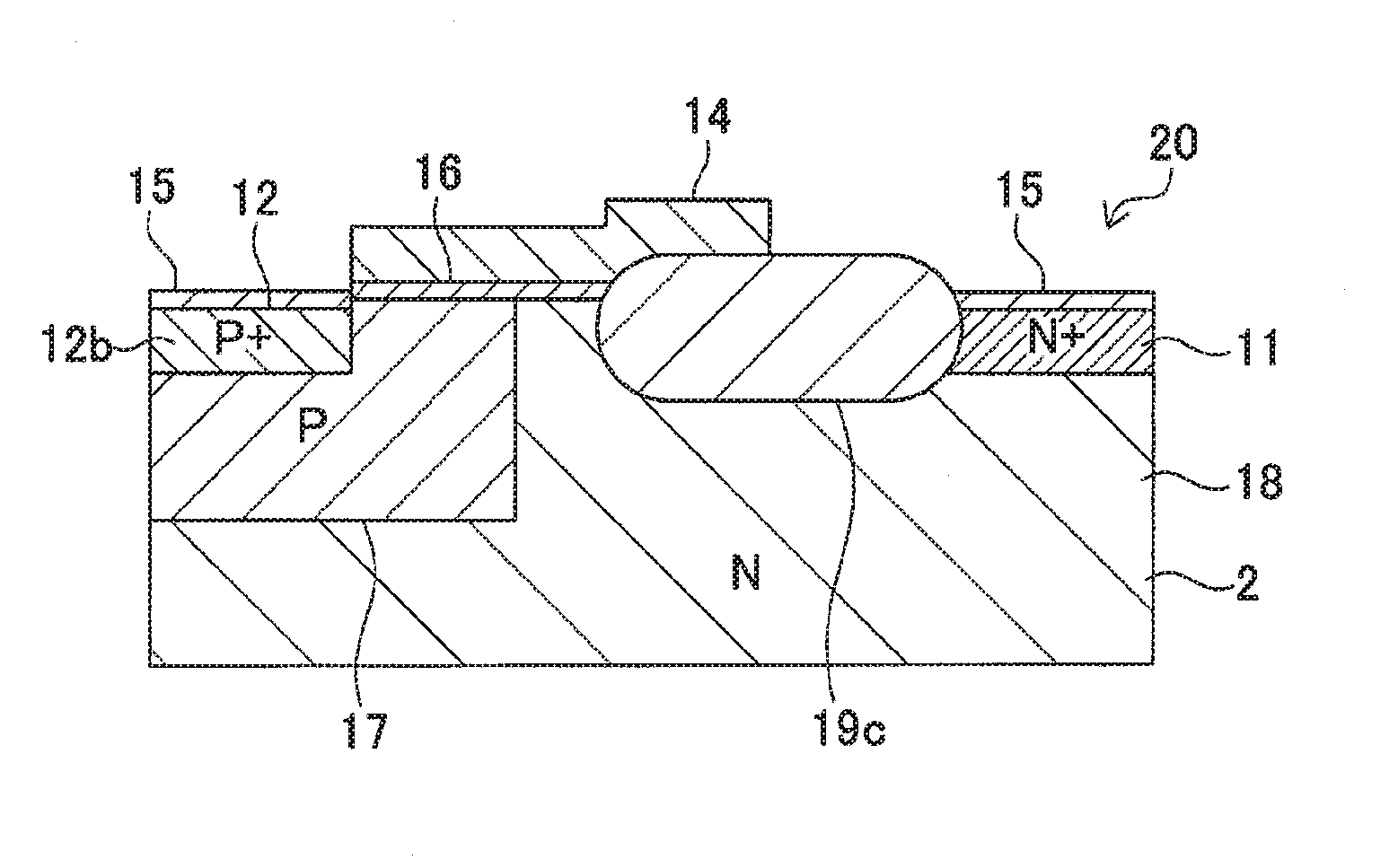
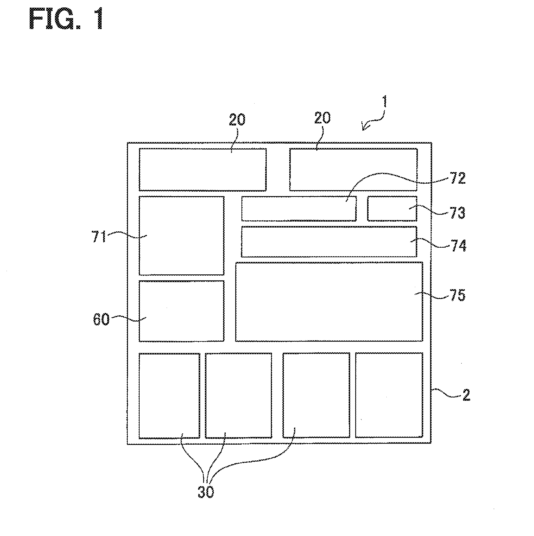
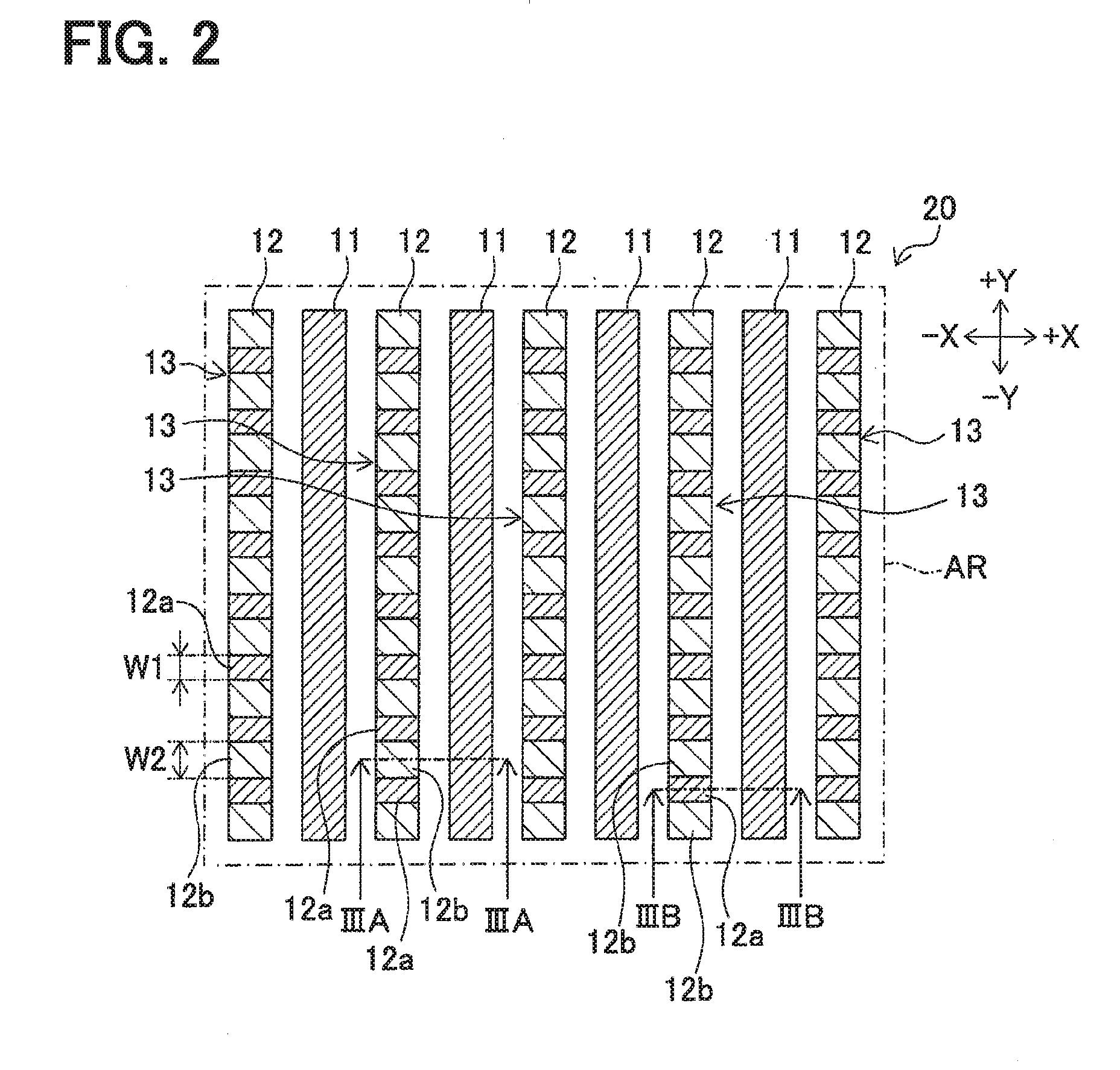
[0036]In a semiconductor device 1 illustrated in FIG. 1, plural semiconductor elements are provided on a surface 2a side of a semiconductor substrate 2 illustrated in FIGS. 3A, 3B, and the like. In the example of FIG. 1, elements such as a bipolar transistor 71, a resistive element 72, a memory 73, a capacitor 74, and a CMOS 75 are disposed on the semiconductor substrate 2, in addition to semiconductor elements 20, 30, and 60 formed as an LDMOS.
[0037]In this configuration, a known SOI substrate in which an insulating film (not illustrated) is interposed between the semiconductor substrate 2 as an element formation substrate and a support substrate (not illustrated) is used as a substrate constituting the semiconductor device 1. Thus, an n-type silicon substrate is used as the semiconductor substrate 2, a silicon substrate is used as the support su...
second embodiment
[0079]Next, a second embodiment will be described.
[0080]The second embodiment is different from the first embodiment in that any one semiconductor element or plural semiconductor elements is formed as a semiconductor element having a mesh structure as illustrated in FIG. 9A in the semiconductor device 1 illustrated in FIG. 1. Otherwise, the second embodiment is the same as the semiconductor device 1 according to the first embodiment.
[0081]A semiconductor element 40 illustrated in FIG. 9A is formed as an LDMOStransistor of a so-called mesh structure. This semiconductor element 40 has a lattice-like structure in which second region portions 12 functioning as a source region are extended in a vertical direction and a transverse direction. FIG. 9A partially illustrates a portion of the semiconductor element 40. However, in practice, the number of longitudinal regions 45 and transverse regions 46 constituting the second region portion 12 is greater than in the configuration of FIG. 9A. ...
third embodiment
[0093]Next, a third embodiment will be described.
[0094]A semiconductor element 50 illustrated in FIG. 10 is formed as a horizontal IGBT. In the semiconductor element 50, a first region portion 51 and a second region portion 52 are alternately formed in a surface layer portion of an N-type semiconductor substrate 2. The first region portion 51 is a region corresponding to a collector of the IGBT and the second region portion 52 is a region corresponding to an emitter of the IGBT. The third embodiment is different from the first embodiment in that any one semiconductor element or plural semiconductor elements are formed as the semiconductor element 50 as illustrated in FIG. 10 in the semiconductor device 1 according to the first embodiment. Otherwise, the third embodiment is the same as the semiconductor device 1 according to the first embodiment.
[0095]As illustrated in FIGS. 10, 11A, and 11B, the first region portion 51 is formed as a P-conductive type semiconductor region which is e...
PUM
Abstract
A semiconductor device includes a semiconductor substrate and a semiconductor element arranged on a predetermined surface side of the semiconductor substrate. The semiconductor element includes: a first region portion at which a first conductivity type semiconductor region is arranged on the surface side of the semiconductor substrate; a second region portion at a position separated from the first region portion; and a gate electrode arranged between the first region portion and the second region portion through an insulating film. In the first region portion, a first conductivity type semiconductor region is arranged. In the second region portion, a first conductivity type semiconductor region and a second conductivity type semiconductor region are alternately arranged. The semiconductor structure portions with a variety of types having ratios of the first conductivity type semiconductor region to the second conductivity type semiconductor region different from each other are provided at the second region portion.
Description
CROSS REFERENCE TO RELATED APPLICATION[0001]This application is based on Japanese Patent Application No. Japanese Patent Application No. 2013-147634 filed on Jul. 16, 2013 and Japanese Patent Application No. 2014-122673 filed on Jun. 13, 2014, the disclosure of which is incorporated herein by reference.TECHNICAL FIELD[0002]The present disclosure relates to a semiconductor device.BACKGROUND ART[0003]A semiconductor device, for example, as disclosed in Patent Literature 1 is provided as a lateral semiconductor device such as an LDMOS. In an example of FIG. 1 in Patent Literature 1, an N-conductive type drain region 104 and a source region 106 are provided on a surface side of a semiconductor substrate. In the source region 106, an N-conductive type diffusion region and a P-conductive type diffusion region are alternately disposed. A gate electrode 109 is disposed between the drain region and the source region through an insulating film on the semiconductor substrate.PRIOR ART LITERATU...
Claims
Application Information
Patent Timeline
Application Date:The date an application was filed.
Publication Date:The date a patent or application was officially published.
First Publication Date:The earliest publication date of a patent with the same application number.
Issue Date:Publication date of the patent grant document.
PCT Entry Date:The Entry date of PCT National Phase.
Estimated Expiry Date:The statutory expiry date of a patent right according to the Patent Law, and it is the longest term of protection that the patent right can achieve without the termination of the patent right due to other reasons(Term extension factor has been taken into account ).
Invalid Date:Actual expiry date is based on effective date or publication date of legal transaction data of invalid patent.

