

Light-emitting device
- Summary
- Abstract
- Description
- Claims
- Application Information
AI Technical Summary
Benefits of technology
Problems solved by technology
Method used
Image

Examples
embodiment 1
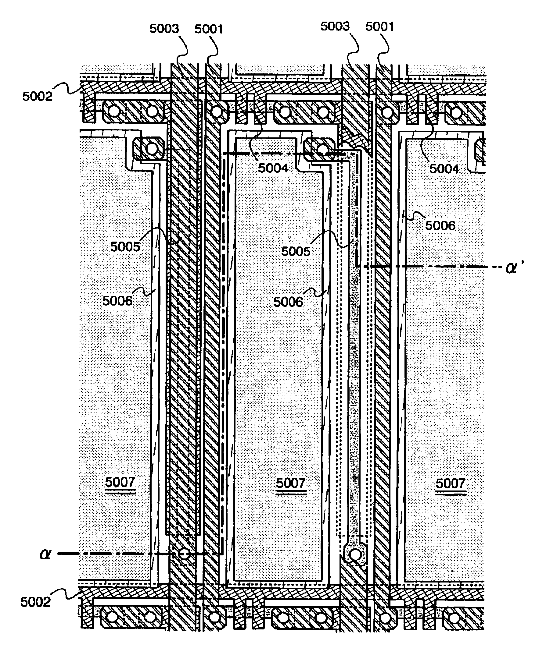
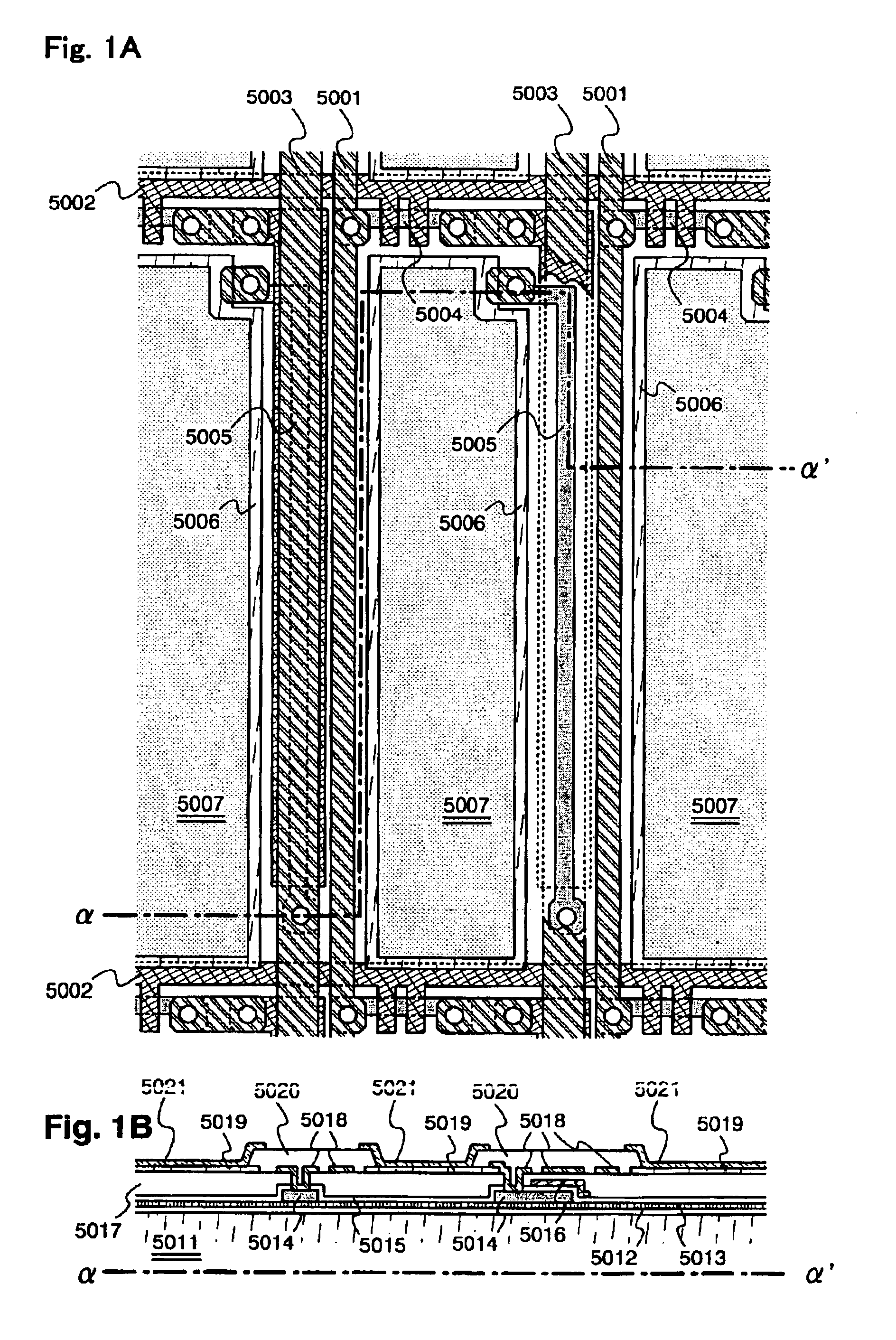
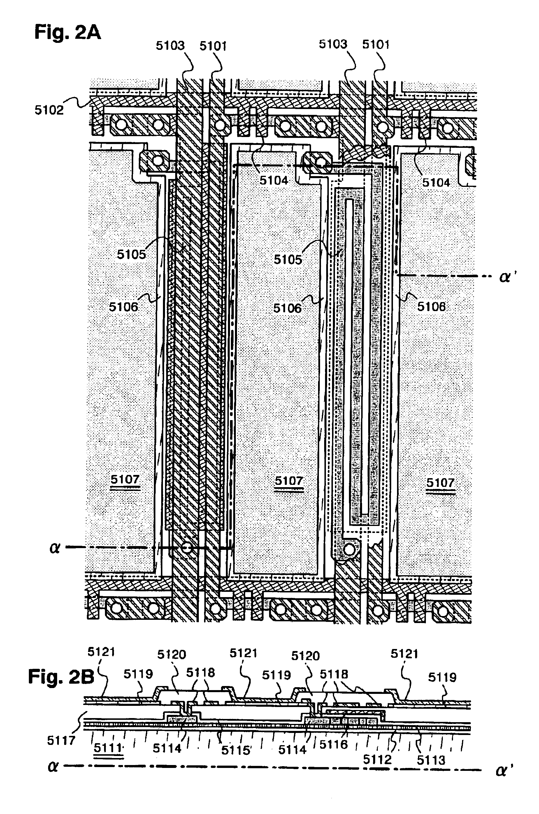
[0076]First, the embodiment will be described with reference to FIG. 1. Here, the light-emitting device produces a full-color display and wherein either the source regions or the drain regions of the driving TFTs of pixels R for emitting light of red color are connected to a current supply line for red color, either the source regions or the drain regions of the driving TFTs of pixels G for emitting light of green color are connected to a current supply line for green color, and either the source regions or the drain regions of the driving TFTs of pixels B for emitting light of blue color are connected to a current feed line for blue color. The EL materials of the EL elements of R, G and B are separately applied like stripes.
[0077]In FIG. 1, the partitioning walls are covering the regions other than the light-emitting areas 5007. Among the partitioning walls 5020, those partitioning walls formed in parallel with the stripes serve as coloring margins. The places where there exist the...
embodiment 2
[0080]When three transistors are used for constituting a pixel, the two transistors, namely, a switching TFT and an erasing TFT, excluding the driving TFT, are linearly arranged to maintain aperture ratio in order to realize a further simplified opening portion. The opening portion of a simple shape which is close to a rectangular shape helps decrease the effect of shrink.
embodiment 3
[0081]In determining the channel length and the channel width of the driving TFT, it is necessary to increase the channel length and the channel width as much as possible and, when the driving TFT is to be operated in the saturated region, to select the channel length to be larger than the channel width, so that the gate-source voltage VGS is little affected by the threshold voltage. Upon increasing the channel length, the characteristics of the driving TFT are more flattened in the saturated region. Here, if the gate-source voltage VGS is increased too much, problems concerning the consumption of electric power and breakdown voltage of the driving TFTs will arise. It is therefore desired that the channel length and the channel width are so adjusted that |VGS| is not lower than 4 V but is not higher than 14 V.
[0082]According to the embodiments 1 to 3, the size of the driving TFT is increased and the channel length L is increased relative to the channel width W, making it possible to...
PUM
 Abstract
Description
Claims
Application Information