Light-emitting device and method of driving the same

a technology of light-emitting devices and light-emitting drivers, which is applied in the direction of static indicating devices, instruments, etc., can solve the problems of obstructing the reduction in the size of the frame, the reduction in the area of the pixel region, and the difficulty in realizing the miniaturization of the signal line driver circuit, etc., to achieve the effect of small area, small frame size, and small area

Inactive Publication Date: 2005-06-21
SEMICON ENERGY LAB CO LTD
View PDF4 Cites 133 Cited by
  • Summary
  • Abstract
  • Description
  • Claims
  • Application Information

AI Technical Summary

Benefits of technology

[0009]The present invention has been made in view of the above, and therefore has an object to provide a novel driving method for conducting gradation display with a circuit structure in which a current source circuit is provided to each signal line. Further, another object of the present invention is to attain miniaturization and reduction in size of a frame of a light-emitting device with the use of a signal line driver circuit that includes a current source circuit having a small area.
[0013]According to the driving method of the present invention, the proportion of the signal line driver circuit to the light-emitting device can be reduced, and thus, the reduction in size of a frame can be attained with a relatively large area of the pixel region to the light-emitting device.
[0014]Further, according to the present invention, provided is a light-emitting device in which each input line for an image signal current is shared by plural current source circuits. Thus, as to the light-emitting device, the number of input terminals (wirings) for image signals can be significantly reduced, and therefore, mounting of a peripheral IC chip becomes easy to be performed. Also, degradation in yield due to connection failure in a connecting portion of an FPC can be avoided.

Problems solved by technology

Thus, the area of the current source circuit shown in FIG. 10C is large, and miniaturization of the signal line driver circuit is difficult to be realized.
As a result, in the light-emitting device, the proportion of the signal line driver circuit is large, which obstructs reduction in size of a frame and leads to reduction in area of the pixel region.

Method used


Image

  • Light-emitting device and method of driving the same
  • Light-emitting device and method of driving the same
  • Light-emitting device and method of driving the same

Examples


embodiment mode 1

[Embodiment Mode 1]

[0029]FIG. 5 shows an example of a signal line driver circuit according to the present invention. Note that FIG. 5 shows a peripheral portion of current source circuits A1, A2, . . . , A(n−1), An.

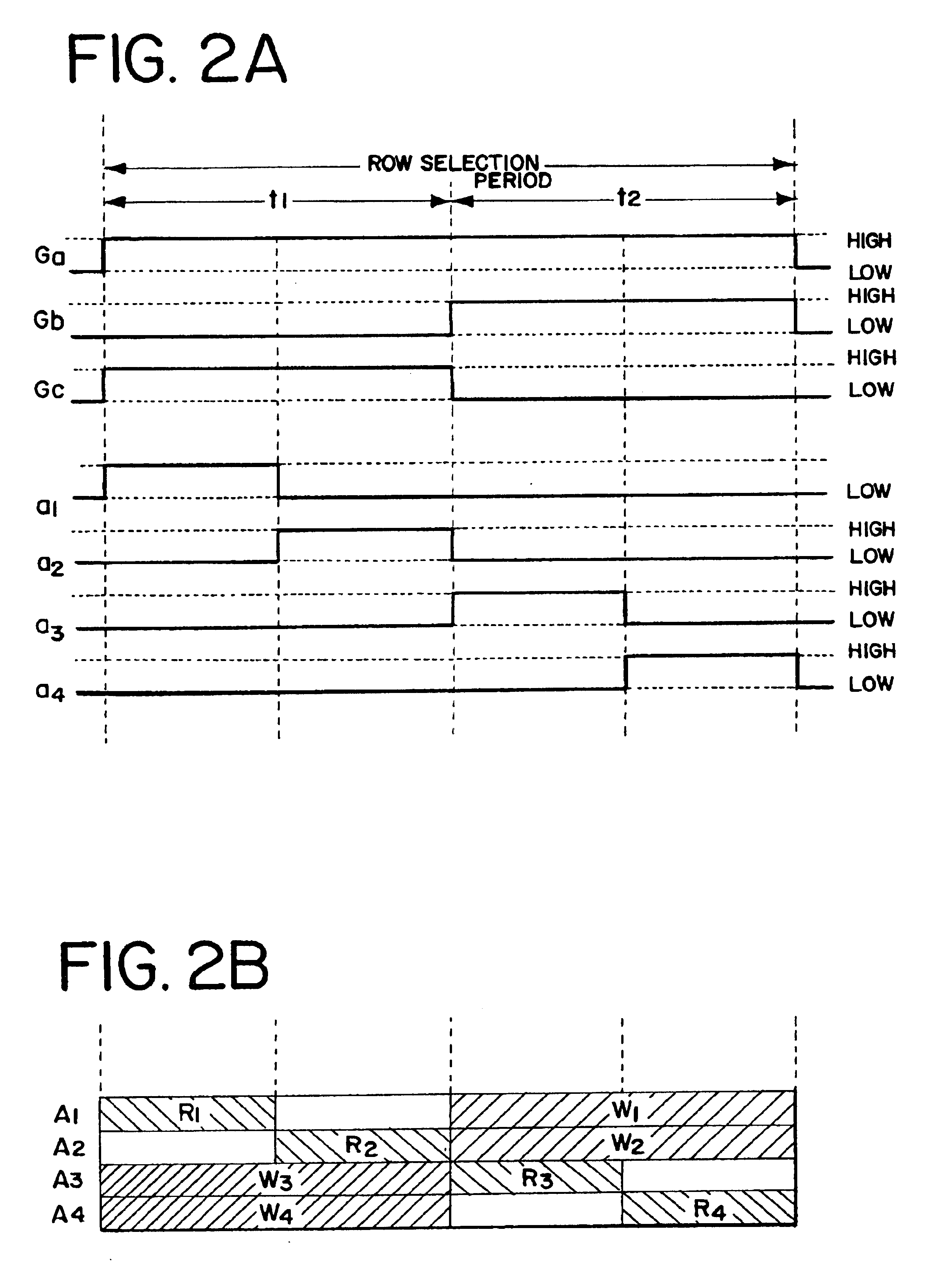
[0030]The signal line driver circuit has the current source circuits A1, A2, . . . , A(n−1), An and an image signal input switches (Sw) on / off of which is controlled by control signals a1, a2, . . . , a(n−1), an. The current source circuits A1, A2, . . . , A(n−1), An output an image signal current to signal lines S1, S2, . . . , S(n−1), Sn, respectively. In a pixel portion, a first scanning line (Ga) and second and third scanning lines (Gb, Gc) are provided so as to be substantially perpendicular to the signal lines S, and pixels are arranged in matrix. Each of the pixels is provided with a pixel switch transistor (Tr1) and a current storage transistor (Tr2).

[0031]The current source circuits are connected with the signal lines and the image signal input switches (Sw), res...

embodiment 1

[Embodiment 1]

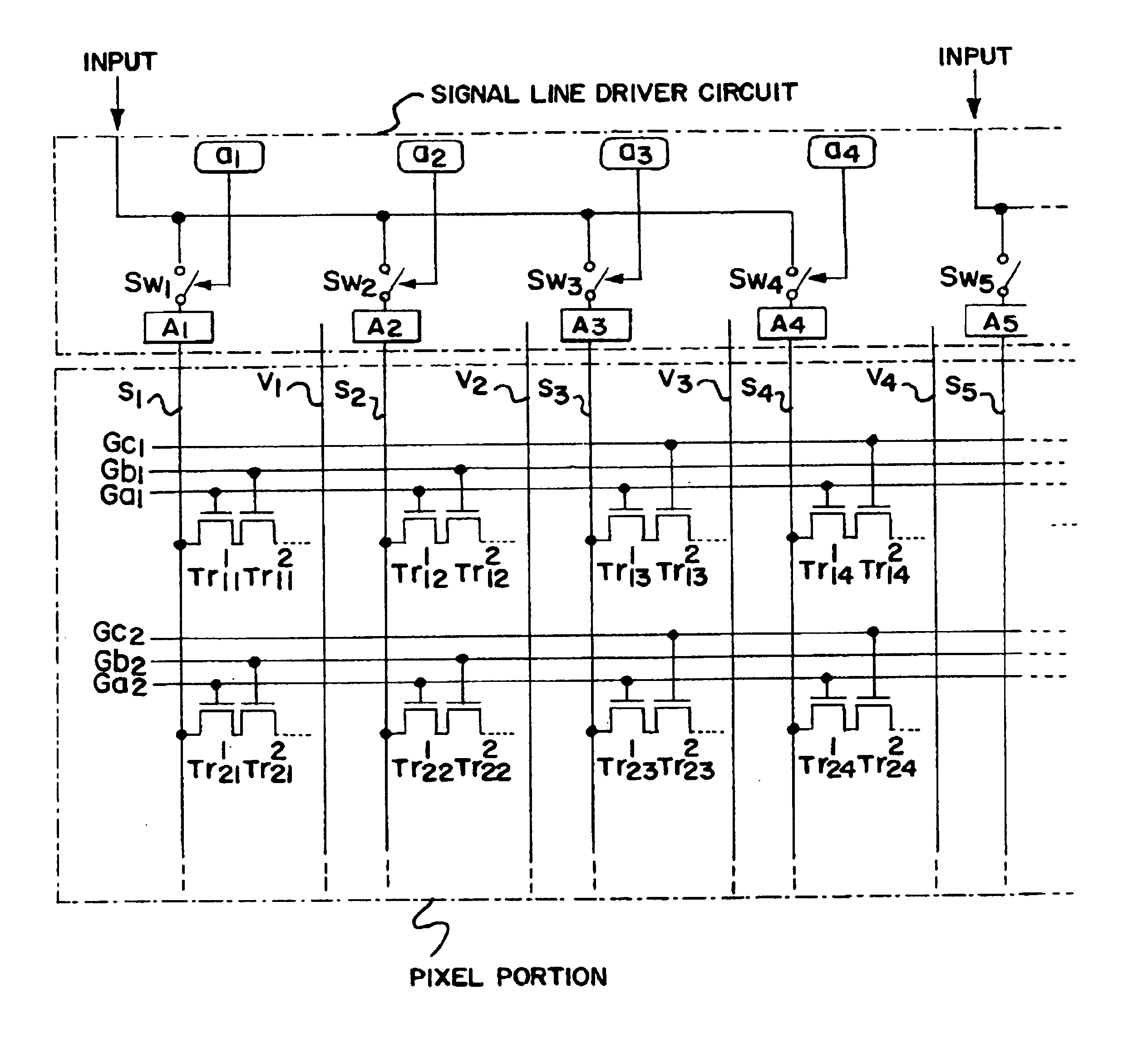
[0054]In this embodiment, description will be made of a structure and a driving method in the case where each input line for an image signal current is shared by four current source circuits. Also, the circuits described with reference to FIGS. 7A and 7B and FIGS. 8A and 8B may be used for a pixel structure and a constant current source in this embodiment. However, the present invention is not limited to the circuits in FIGS. 7A and 7B and FIGS. 8A and 8B.

[0055]FIG. 1 shows a structure in which each input line for image signals is shared by four current source circuits. In FIG. 1, current source circuits A1, A2, . . . , image signal input switches Sw1, Sw2, . . . on / off of which is controlled by control signals a1, a2, . . . , and signal lines S1, S2, . . . are provided. Then, the first scanning line (Ga) and the second and third scanning lines (Gb), (Gc) are provided so as to be substantially perpendicular to the respective signal lines, and each pixel is arranged at ...

embodiment 2

[Embodiment 2]

[0062]In this embodiment, description will be made of a structure and a driving method in the case where each input line for an image signal is shared by eight current source circuits. Also, the circuits described with reference to FIGS. 7A and 7B and FIGS. 8A and 8B are used for a pixel structure and a constant current source in this embodiment. However, the present invention is not limited to the circuits in FIGS. 7A and 7B and FIGS. 8A and 8B.

[0063]FIG. 3 shows a structure in which each input line for image signals is shared by eight current source circuits. In FIG. 3, current source circuits A1, A2, . . . , image signal input switches on / off of which is controlled by control signals a1, a2, . . . , and signal lines S1, S2, . . . are provided. Then, the first scanning line (Ga) and the second and third scanning lines (Gb), (Gc) are provided so as to be substantially perpendicular to the respective signal lines, and each pixel is arranged at an intersecting point of ...


PUM


Abstract

A novel driving method for conducting gradation display is provided. Also, a signal line driver circuit is provided which includes a current source circuit having a small area. Further, miniaturization and reduction in size of a frame of a light-emitting device can be attained. A gate selection period is divided into plural periods, and a (writing) operation of writing a signal to a pixel having a transistor connected with a scanning line that is selected and a (reading) operation of reading a signal current into a current source circuit connected with a signal line connected with a scanning line that is not selected are performed simultaneously in each of the divided periods in the gate selection period. Therefore, the signal line driver circuit that includes a current source circuit having a small area is provided. Consequently, the miniaturization and reduction in size of the frame of the light-emitting device can be attained.

Description

BACKGROUND OF THE INVENTION[0001]1. Field of the Invention[0002]The present invention relates to techniques for a semiconductor integrated circuit and its driving method. The invention also relates to a light-emitting device that has a semiconductor integrated circuit of the present invention in its driver circuit portion and a pixel portion. In particular, the present invention relates to an active matrix type light-emitting device in which the semiconductor integrated circuit of the present invention is applied to a signal line driver circuit of the driver circuit portion.[0003]2. Description of the Related Art[0004]In recent years, research and development of light-emitting devices using self-light-emitting elements such as organic light-emitting diodes (OLEDs) have progressed. An OLED has an anode and a cathode, and has a structure in which an organic compound layer is sandwiched between the aforementioned anode and cathode. Light-emitting devices using OLEDs have characteristic...

Claims


Application Information

Patent Timeline
Patent Type & Authority Patents(United States)
IPC IPC(8): G09G3/32G09G3/20
CPCG09G3/325G09G3/3283G09G3/20G09G2310/0275G09G2300/0842G09G2300/0861G09G2300/0814
Inventor INUKAI, KAZUTAKA
Owner SEMICON ENERGY LAB CO LTD
Why Eureka
Try Eureka