Contact for use in an integrated circuit and a method of manufacture therefor

a technology for integrated circuits and contacts, applied in the field of contacts, can solve problems such as voids, electromigration and reliability failures, and tungsten seams, and achieve the effects of increasing yield and reliability failures, reducing the number of contacts, and improving the quality of conta

Inactive Publication Date: 2005-06-28
BELL SEMICON LLC
View PDF3 Cites 115 Cited by
  • Summary
  • Abstract
  • Description
  • Claims
  • Application Information

AI Technical Summary

Problems solved by technology

Micro-miniaturization of semiconductor devices has resulted in higher performance, through increases in transistor speed and in the number of devices incorporated in a chip; however, this trend has also increased yield and reliability failures.
With a higher aspect ratio, the use of aluminum-based metallization to fill the contact opening, results in electromigration and reliability failures.
Unfortunately, after tungsten plug filling, voids, or so-called tungsten seams, are often observed in the tungsten material.
Moreover, in certain situations the size of the tungsten seam is increased due to exposure to the removal process.
This often creates a difficult topology for subsequent metallization coverage as well as electrical device degradation, which is especially apparent as leakage in metal-oxide-metal MOM capacitor structures.
The tapered via profile helps reduce many of the tungsten seam issues, however, it often leads to increased contact resistance, which is also very undesirable.

Method used


Image

  • Contact for use in an integrated circuit and a method of manufacture therefor
  • Contact for use in an integrated circuit and a method of manufacture therefor
  • Contact for use in an integrated circuit and a method of manufacture therefor

Examples


Embodiment Construction

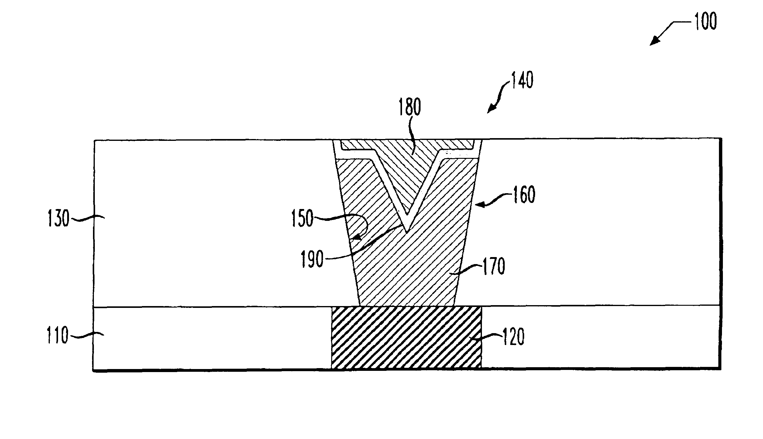
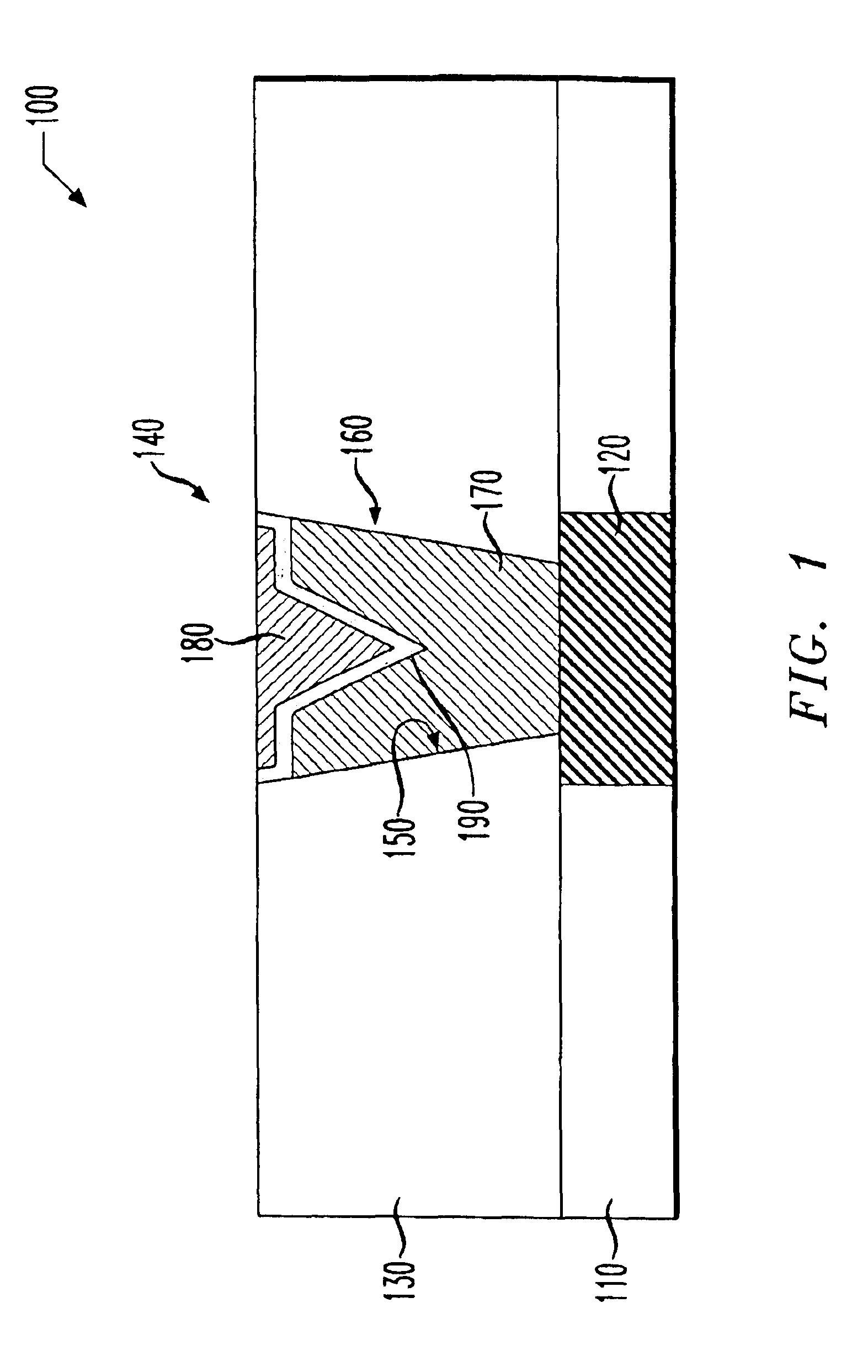
[0019]Referring initially to FIG. 1, illustrated is a cross-sectional view of one embodiment of a portion of an integrated circuit 100 constructed according to the principles of the present invention. In the embodiment illustrated in FIG. 1, the integrated circuit 100 includes a dielectric layer 110 having a conductive feature 120 located therein. The dielectric layer 110 might be an interlevel dielectric layer and the conductive feature 120 might be a runner located within the dielectric layer 110 for connecting various features in the integrated circuit 100. Other dielectric layers and conductive features are within the scope of the present invention.

[0020]Located over the dielectric layer 110 and the conductive feature 120 is a substrate 130. The substrate 130, similar to the dielectric layer 110, may comprise an interlevel dielectric layer. However, the substrate 130 may comprise other layers and stay within the scope of the present invention. Located within the substrate 130 an...


PUM


Abstract

The present invention provides a contact for use in an integrated circuit, a method of manufacture therefor, and an integrated circuit including the aforementioned contact. The contact, in accordance with the principles of the present invention, may include a via located in a substrate, and a contact plug located in the via, wherein the contact plug has a first portion having a notch removed therefrom and a second portion filling the notch.

Description

TECHNICAL FIELD OF THE INVENTION[0001]The present invention is directed, in general, to a contact and, more specifically, to a contact for use in an integrated circuit, a method of manufacture therefor, and an integrated circuit including the contact.BACKGROUND OF THE INVENTION[0002]Devices in the semiconductor industry continue to advance toward higher performance, while maintaining or even lowering the cost of manufacturing. Micro-miniaturization of semiconductor devices has resulted in higher performance, through increases in transistor speed and in the number of devices incorporated in a chip; however, this trend has also increased yield and reliability failures. As contact or via openings decrease in size, the aspect ratio, or the ratio of the depth of the opening to the diameter of the opening, also increases. With a higher aspect ratio, the use of aluminum-based metallization to fill the contact opening, results in electromigration and reliability failures. To alleviate relia...

Claims


Application Information

Patent Timeline
Patent Type & Authority Patents(United States)
IPC IPC(8): H01R13/28H01R13/02H01R25/00H01L21/768
CPCH01L21/76877
Inventor LAYADI, NACEMAURY, ALVARO
Owner BELL SEMICON LLC
Why Eureka
Try Eureka