Using scatterometry to obtain measurements of in circuit structures

a scatterometry and circuit technology, applied in semiconductor/solid-state device testing/measurement, instruments, photomechanical equipment, etc., can solve problems such as adversely affecting chip reliability and compromising electrically active regions performance, and achieve the effect of reducing sacrificing valuable chip real estate and rapid inspection

Inactive Publication Date: 2005-06-28
GLOBALFOUNDRIES INC
View PDF5 Cites 9 Cited by
  • Summary
  • Abstract
  • Description
  • Claims
  • Application Information

AI Technical Summary

Benefits of technology

[0005]According to one or more aspects of the present invention, measurements of repeating in circuit structures formed on a wafer during a semiconductor fabrication process are taken by a system employing scatterometry based techniques. The measurements can be utilized to generate feed forward and / or feedback control data that can utilized to selectively adjust one or more fabrication components and / or operating parameters associated therewith to achieve desired results (e.g., critical dimensions within acceptable tolerances and / or mitigation of overlay). Additionally, the measurements can be employed in determining whether to discard the wafer or portions thereof based on a cost benefit analysis, for example. Directly measuring in circuit structures mitigates sacrificing valuable chip real estate as test grating structures may not need to be formed within the wafer.

Problems solved by technology

If the layers are not aligned within acceptable tolerances, overlay errors can occur compromising the performance of the electrically active regions and adversely affecting chip reliability.

Method used


Image

  • Using scatterometry to obtain measurements of in circuit structures
  • Using scatterometry to obtain measurements of in circuit structures
  • Using scatterometry to obtain measurements of in circuit structures

Examples


Embodiment Construction

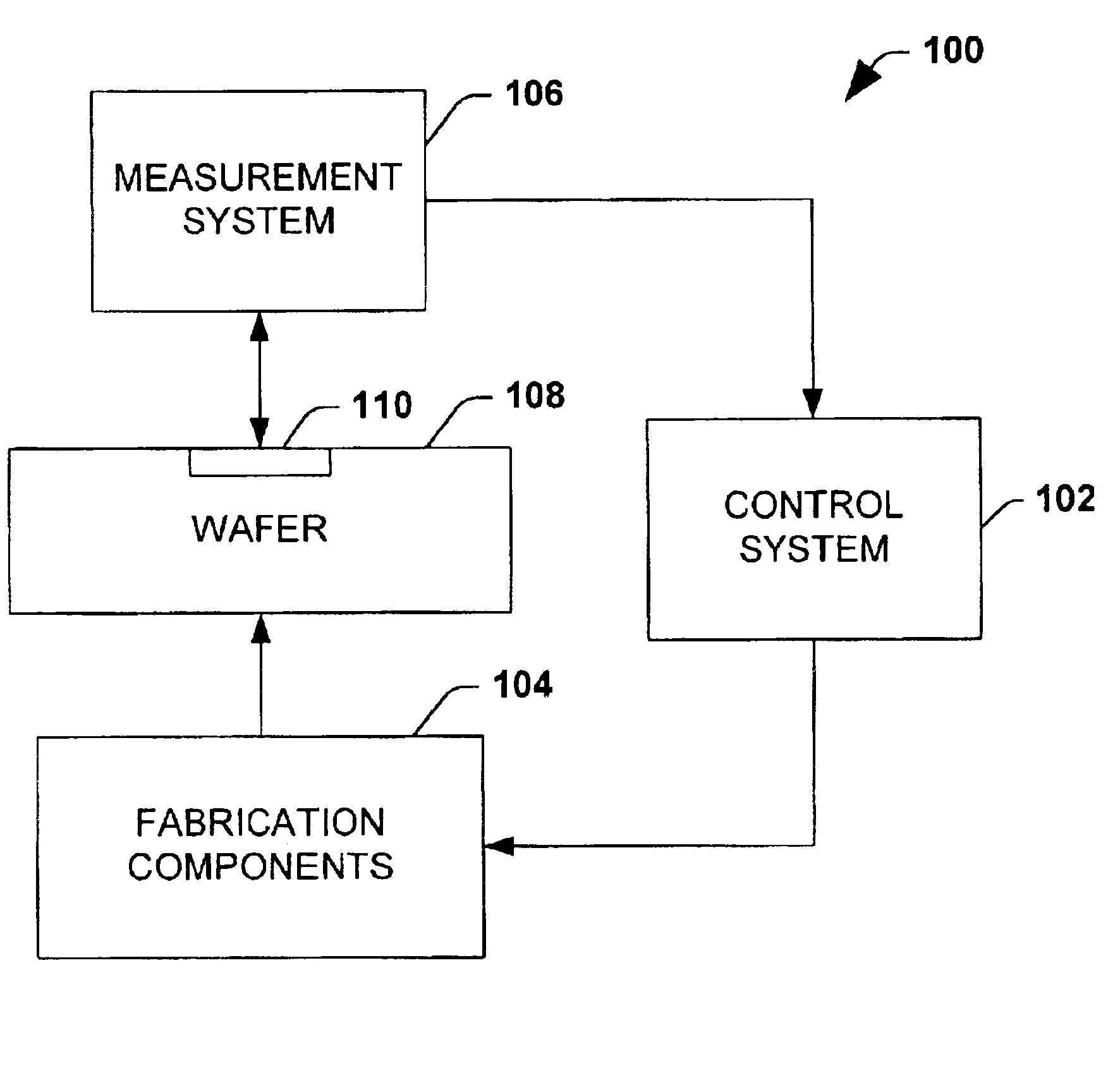
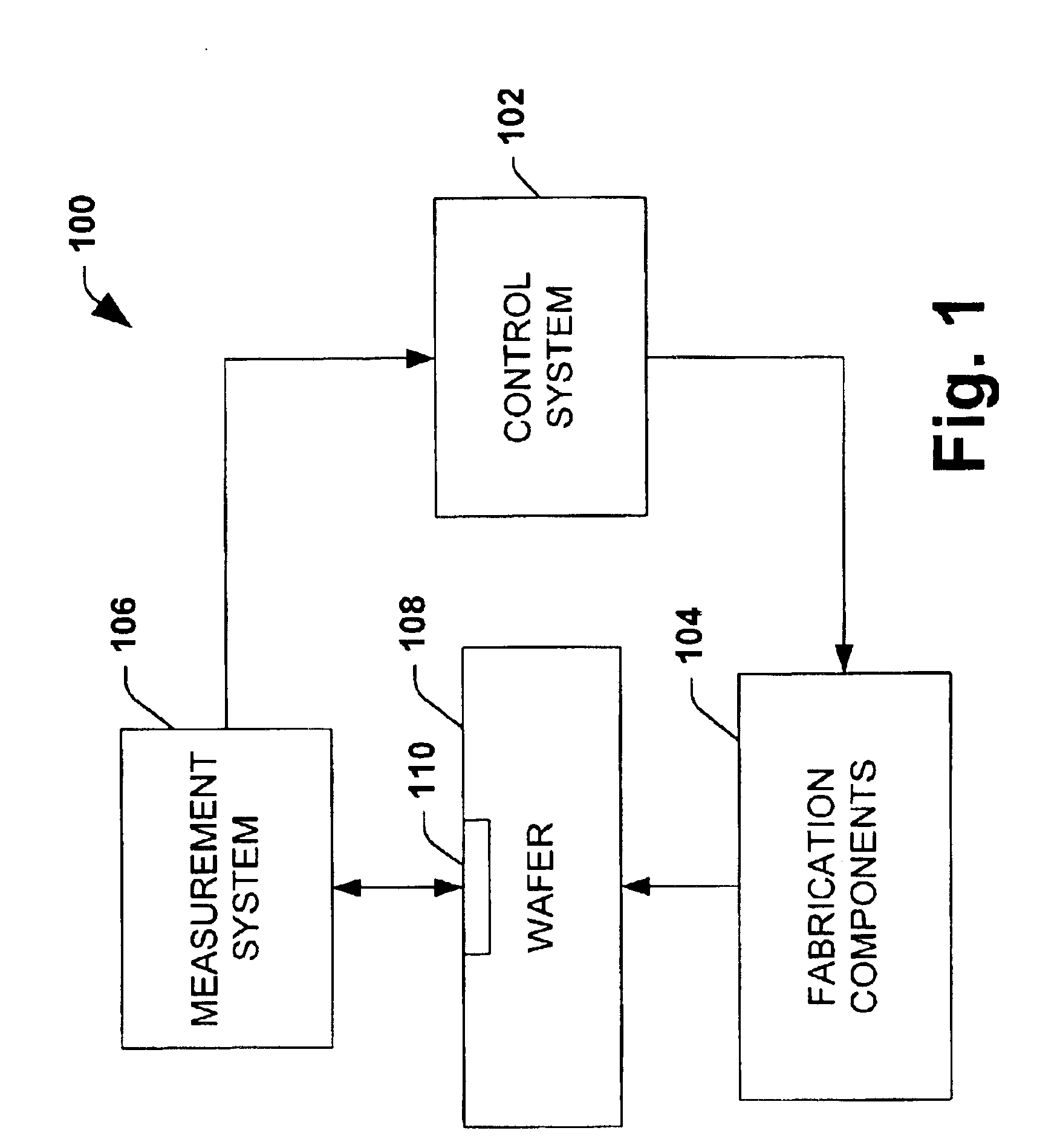
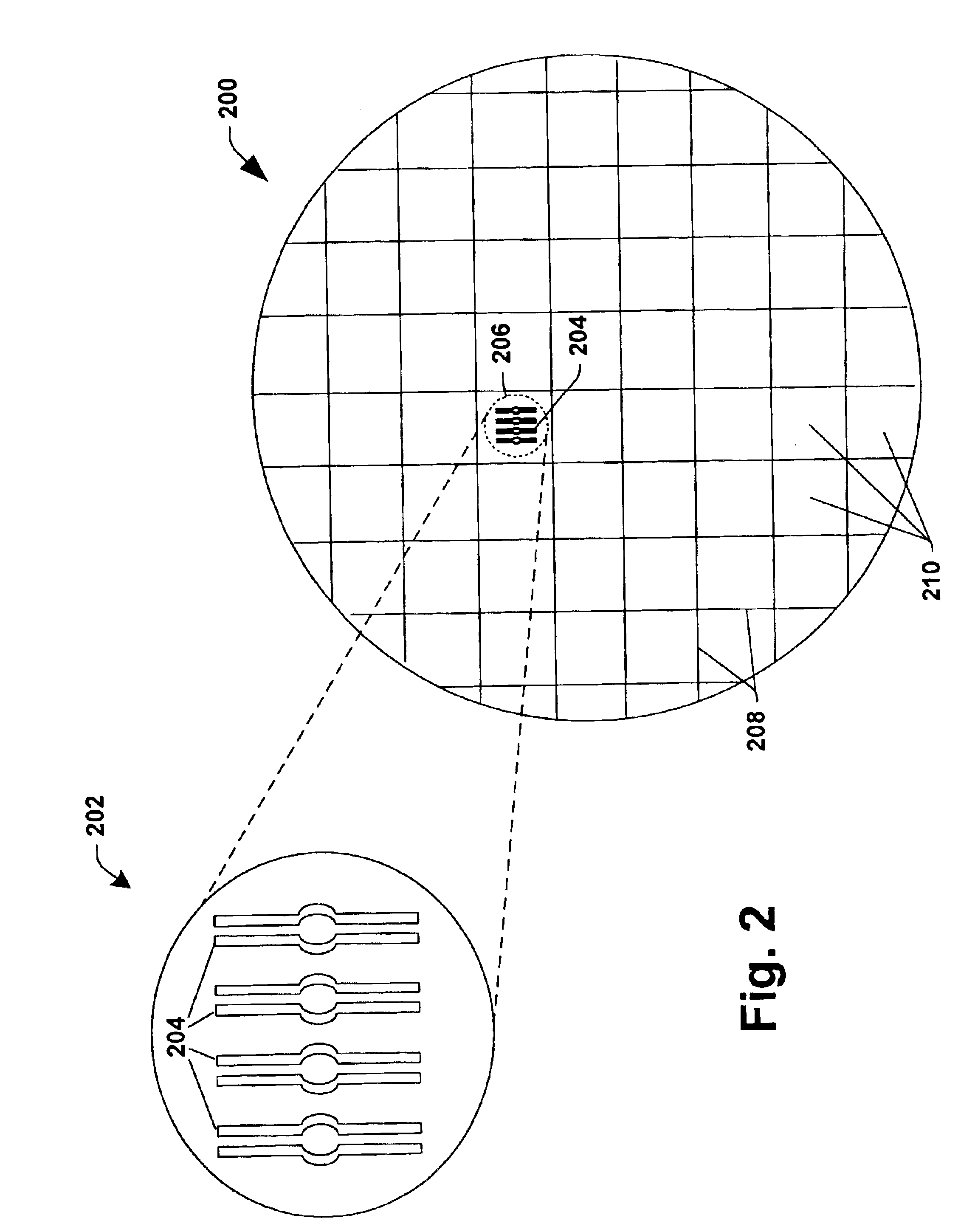
[0025]The present invention is now described with reference to the drawings, wherein like reference numerals are used to refer to like elements throughout. In the following description, for purposes of explanation, numerous specific details are set forth in order to provide a thorough understanding of the present invention. It may be evident, however, to one skilled in the art that one or more aspects of the present invention may be practiced with a lesser degree of these specific details. In other instances, well-known structures and devices are shown in block diagram form in order to facilitate describing one or more aspects of the present invention.

[0026]The term “component” as used herein includes computer-related entities, either hardware, a combination of hardware and software, software, or software in execution. For example, a component may be a process running on a processor, a processor, an object, an executable, a thread of execution, a program and a computer. By way of il...


PUM

PropertyMeasurementUnit
wavelengthsaaaaaaaaaa
semiconductoraaaaaaaaaa
circuit structuresaaaaaaaaaa

Abstract

A system and methodology are disclosed for monitoring and controlling a semiconductor fabrication process. Measurements are taken in accordance with scatterometry based techniques of repeating in circuit structures that evolve on a wafer as the wafer undergoes the fabrication process. The measurements can be employed to generate feed forward and / or feedback control data that can utilized to selectively adjust one or more fabrication components and / or operating parameters associated therewith to adapt the fabrication process. Additionally, the measurements can be employed in determining whether to discard the wafer or portions thereof based on a cost benefit analysis, for example. Directly measuring in circuit structures mitigates sacrificing valuable chip real estate as test grating structures may not need to be formed within the wafer, and also facilitates control over the elements that actually affect resulting chip performance.

Description

TECHNICAL FIELD[0001]The present invention generally relates to monitoring and / or controlling a semiconductor fabrication process, and in particular to a system and methodology for obtaining measurements of in circuit structures forming during the fabrication process and controlling the fabrication process in response to the measurements.BACKGROUND[0002]In the semiconductor industry, there is a continuing trend toward higher device densities. To achieve these high densities, there has been and continues to be efforts toward scaling down device dimensions (e.g., at submicron levels) on semiconductor wafers. In order to accomplish such high device packing density, smaller and smaller feature and structure sizes are required in integrated circuits (ICs) fabricated on small rectangular portions of the wafer, commonly known as dies. This may include the width and spacing of interconnecting lines, spacing and diameter of contact holes, the surface geometry such as corners and edges of var...

Claims


Application Information

Patent Timeline
Patent Type & Authority Patents(United States)
IPC IPC(8): H01L21/66G01N21/47
CPCG01N21/4738H01L22/20H01L2924/0002H01L2924/00H01L22/00
Inventor CHOO, BRYAN K.SINGH, BHANWARSUBRAMANIAN, RAMKUMARRANGARAJAN, BHARATH
Owner GLOBALFOUNDRIES INC
Why Eureka
Try Eureka