
Non-volatile semiconductor memory that is based on a virtual ground method

Inactive Publication Date: 2005-07-05
INFINEON TECH LLC
View PDF4 Cites 2 Cited by
  • Summary
  • Abstract
  • Description
  • Claims
  • Application Information

AI Technical Summary

Benefits of technology

[0024]The present invention was made under the background circumstances as described above. An object of the present invention is to provide a semiconductor memory in which a decrease in reading margin at the time of a memory being read is prevented.

Problems solved by technology

However, the conventional semiconductor memory 30 has the following problems.

Method used


Image

  • Non-volatile semiconductor memory that is based on a virtual ground method
  • Non-volatile semiconductor memory that is based on a virtual ground method
  • Non-volatile semiconductor memory that is based on a virtual ground method

Examples


Embodiment Construction

[0034]Embodiments of the present invention will now be described with reference to the drawings.

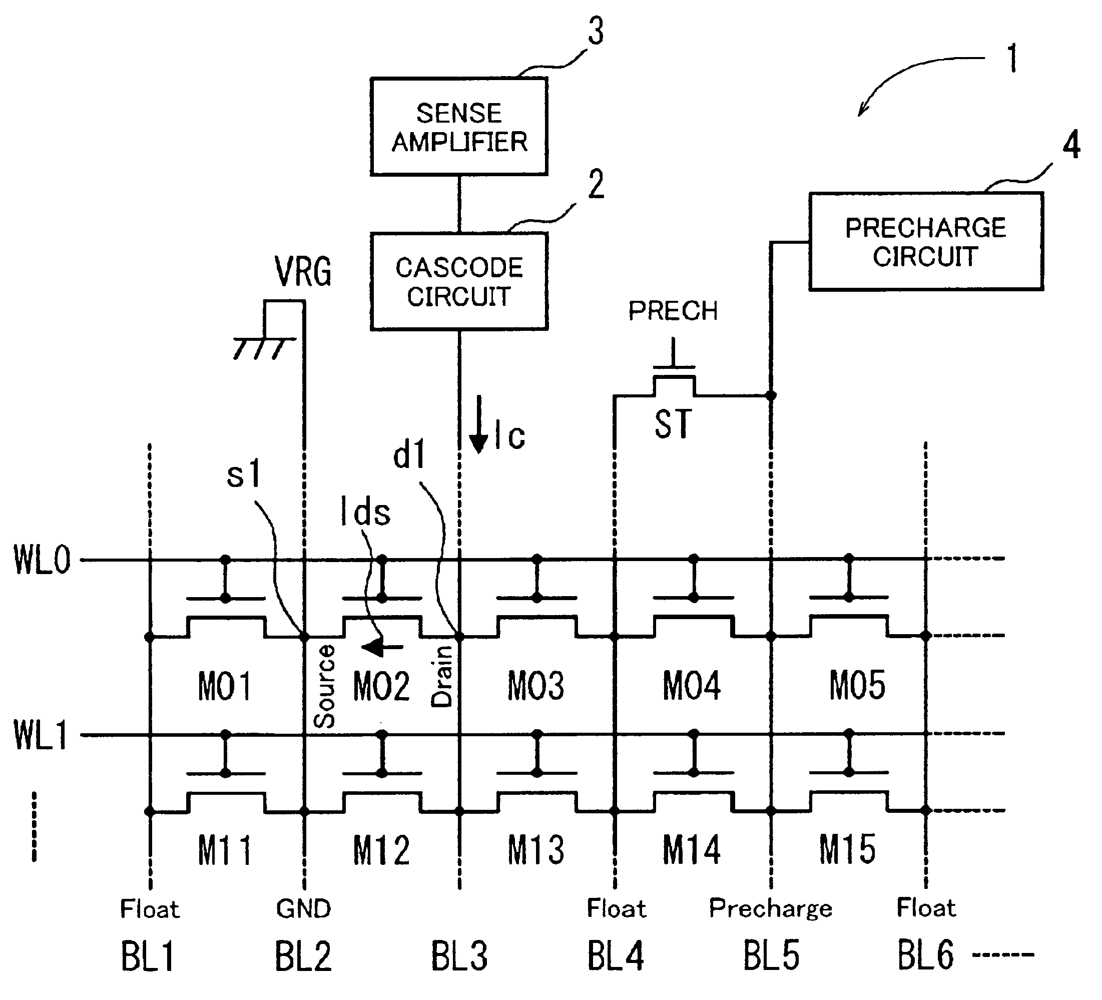
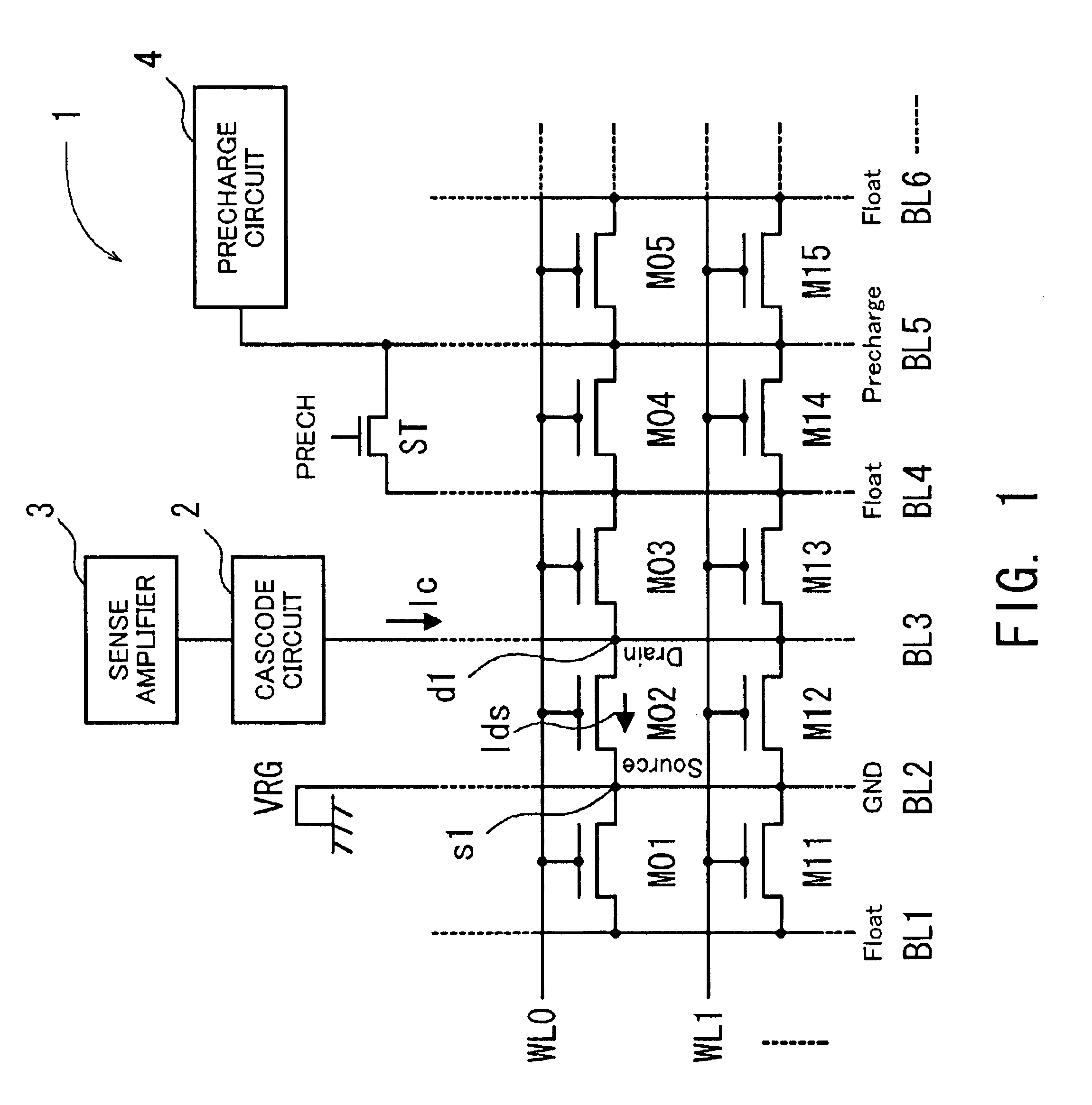
[0035]FIG. 1 is a view showing the rough structure of a semiconductor memory according to the present invention.

[0036]A semiconductor memory 1 includes a plurality of memory cells Mmn (“m” is a natural number and “n” is a natural number except zero) arranged like a matrix. There are word lines WLm (this “m” corresponds to “m” in the memory cells “Mmn”) which are connected to gates of the memory cells Mmn and bit lines BLn (this “n” corresponds to “n” in the memory cells “Mmn”) which are intersecting the word lines WLm and which are connected to sources or drains of the memory cells Mmn. These memory cells Mmn, word lines WLm, and bit lines BLn form a memory cell array.

[0037]Moreover, to write data to or read data from the memory cells Mmn, the semiconductor memory 1 includes a cascode circuit 2 having a current source for supplying an electric current to the memory cells Mmn, a sense ampl...


PUM


Abstract

A semiconductor memory that prevents a decrease in margin at read time. A bit line in a floating state between a drain in a memory cell to be read and a charged bit line is charged for a certain period of time.

Description

CROSS-REFERENCE TO RELATED APPLICATIONS[0001]This application is based upon and claims priority of Japanese Patent Application No. 2002-080554, filed on Mar. 22, 2002, the contents being incorporated herein by reference.BACKGROUND OF THE INVENTION[0002](1) Field of the Invention[0003]This invention relates to a semiconductor memory and, more particularly, to a nonvolatile semiconductor memory based on a virtual ground method.[0004](2) Description of the Related Art[0005]In recent years large-capacity and highly-integrated memories have been required. As a result, nonvolatile semiconductor memories based on a multi value method, a virtual ground method, and the like in which effective cell area can be reduced have been developed and put to practical use.[0006]Semiconductor memories based on a virtual ground method have a structure in which two memory cells share one bit line, so high integration levels can be attained.[0007]FIG. 5 is a view showing the rough structure of part of a co...

Claims


Application Information

Patent Timeline
IPC IPC(8): G11C16/26G11C16/04G11C16/06G11C16/02
CPCG11C16/0491G11C16/26A47B13/021
Inventor YAMASHITA, MINORUEINAGA, YUICHIKIDO, KAZUNARI
Owner INFINEON TECH LLC
Learn More