Multi-stage output multiplexing circuits and methods for double data rate synchronous memory devices

a synchronous memory device and output multiplexing technology, applied in the field of output multiplexing circuits and methods for semiconductor memory devices, can solve the problems of dq skew, dq skew, and difficulty in high-frequency operations

Active Publication Date: 2005-07-05
SAMSUNG ELECTRONICS CO LTD
View PDF5 Cites 28 Cited by
  • Summary
  • Abstract
  • Description
  • Claims
  • Application Information

AI Technical Summary

Problems solved by technology

As such, it may be difficult to perform high-frequency operations.
Moreover, when an operating frequency increases, CAS latency generally increases.
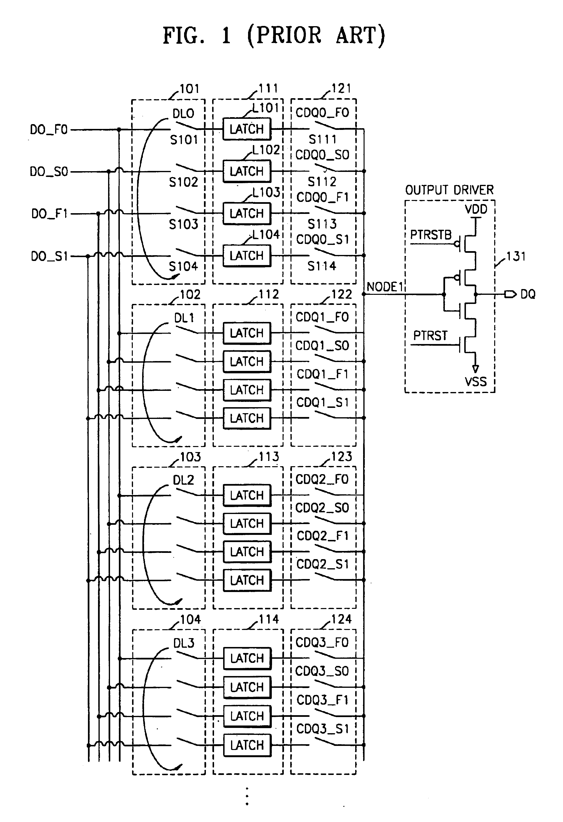
In addition, skew of a CDQi signal at each output terminal DQ may cause DQ skew, i.e., skew between data output to the output terminal DQ.
As a result, the area of the chip may further increase, and in the case of the wide output terminal DQ, it may be difficult to completely reduce the DQ skew.

Method used


Image

  • Multi-stage output multiplexing circuits and methods for double data rate synchronous memory devices
  • Multi-stage output multiplexing circuits and methods for double data rate synchronous memory devices
  • Multi-stage output multiplexing circuits and methods for double data rate synchronous memory devices

Examples


Embodiment Construction

[0023]The present invention now will be described more fully hereinafter with reference to the accompanying drawings, in which embodiments of the invention are shown. This invention may, however, be embodied in many different forms and should not be construed as limited to the embodiments set forth herein. Rather, these embodiments are provided so that this disclosure will be thorough and complete, and will fully convey the scope of the invention to those skilled in the art. Moreover, each embodiment described and illustrated herein includes its complementary conductivity type embodiment as well. Like numbers refer to like elements throughout.

[0024]It will be understood that although the terms first, second, etc. are used herein to describe various elements, these elements should not be limited by these terms. These terms are only used to distinguish one element from another element. Thus, a first element discussed below could be termed a second element, and similarly, a second elem...


PUM


Abstract

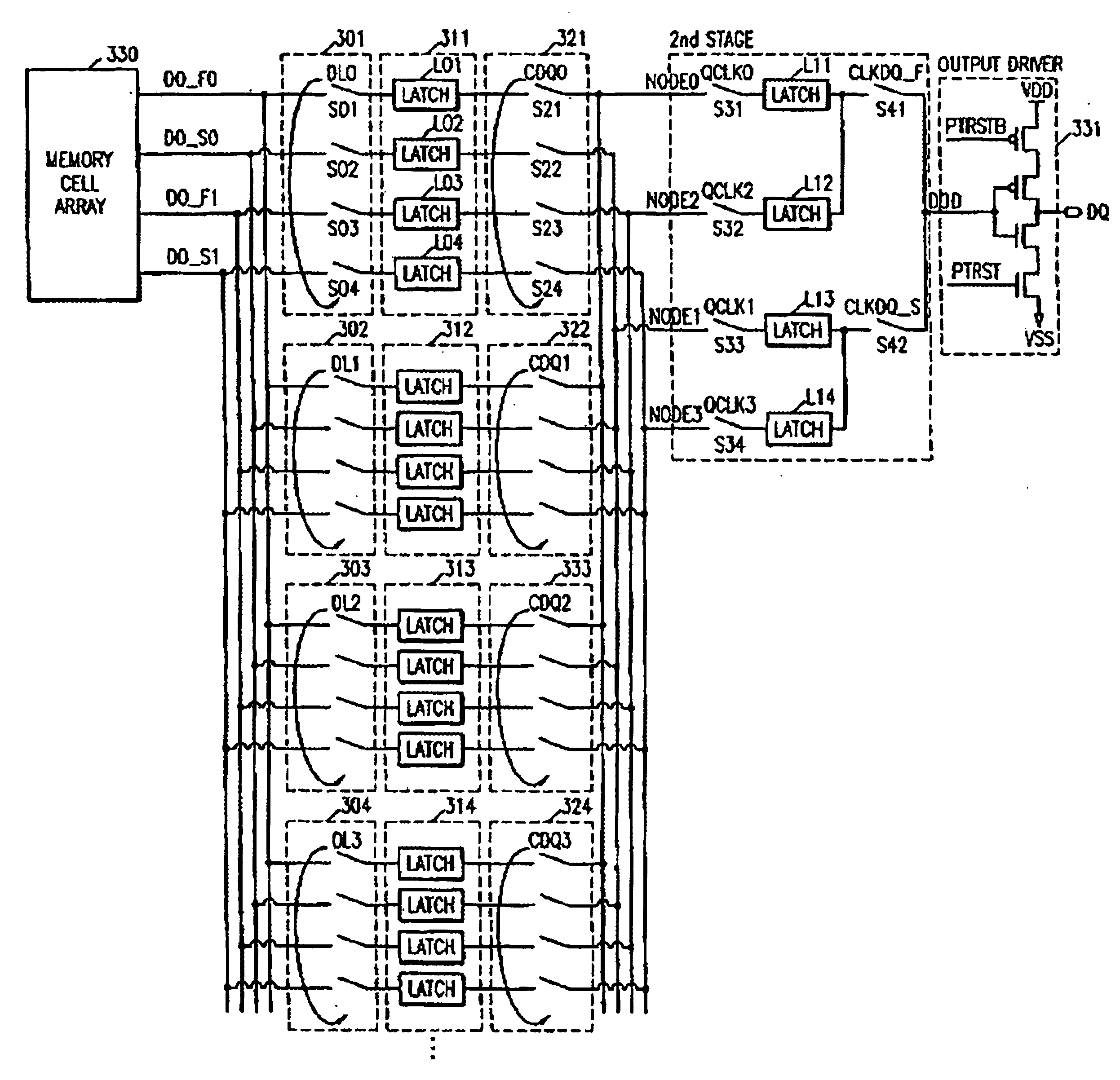
An output multiplexing circuit for a Double Data Rate (DDR) synchronous memory device includes n first latches, n first switches, n second switches, n second latches, and two third switches. The n first latches simultaneously prefetch n-bit data transmitted from a memory cell array via a data path. The n first switches simultaneously transfer the n-bit data prefetched into the first latches to n nodes in response to a CAS latency information signal. The n second switches simultaneously transfer data on the nodes in response to n signals that are synchronized with a clock signal and sequentially generated at a predetermined interval. The n second latches store the data transferred via the second switches. The two third switches sequentially transfer the data stored in the n second latches to an input terminal of an output driver of the memory device at a rising edge and a falling edge of a delay signal of the clock signal. Analogous methods also are described.

Description

RELATED APPLICATION[0001]This application claims the benefit of Korean Patent Application No. 2003-0021037, filed Apr. 3, 2003, the disclosure of which is hereby incorporated herein by reference in its entirety as if set forth fully herein.FIELD OF THE INVENTION[0002]The present invention relates to semiconductor memory devices, and more particularly to output multiplexing circuits and methods for semiconductor memory devices such as Double Data Rate (DDR) synchronous memory devices.BACKGROUND OF THE INVENTION[0003]As the operating frequency of a semiconductor memory device increases, an operating speed inside the semiconductor memory device may be reduced and only an operating frequency of an output portion thereof may be increased, using 2-bit, 4-bit, 8-bit or higher prefetch techniques. Thus, an output multiplexing circuit, which serially transfers internal parallel data to an output terminal, may be installed between the semiconductor memory device and the output portion thereof...

Claims


Application Information

Patent Timeline
Patent Type & Authority Patents(United States)
IPC IPC(8): G11C7/10G11C11/40
CPCG11C7/1012G11C7/1039G11C7/1051G11C7/106G11C7/1072G11C11/40
Inventor LEE, SANG-BO
Owner SAMSUNG ELECTRONICS CO LTD
Why Eureka
Try Eureka