Memory storage device with segmented column line array

a memory storage device and column line array technology, applied in semiconductor devices, digital storage, instruments, etc., can solve the problems of more difficult to detect the difference between non-programmed and programmed configurations, and difficult to accurately read memory

Inactive Publication Date: 2005-07-12
TAIWAN SEMICON MFG CO LTD
View PDF12 Cites 46 Cited by
  • Summary
  • Abstract
  • Description
  • Claims
  • Application Information

AI Technical Summary

Problems solved by technology

Integrated circuit memories often times have higher transistor densities than other types of circuits, and as a result, tend to push the leading edge of the technology envelope.
One disadvantage of the two dimensional ROM arrays are leakage currents which tend to make accurate memory reads more difficult as the number of memory cells in the arrays are increased.
If a particular row and column line are selected and the read voltage is applied, other storage elements positioned along the row line or along the column line can provide leakage currents which make it more difficult to detect the difference between the non-programmed and programmed configurations.

Method used


Image

  • Memory storage device with segmented column line array
  • Memory storage device with segmented column line array
  • Memory storage device with segmented column line array

Examples


first embodiment

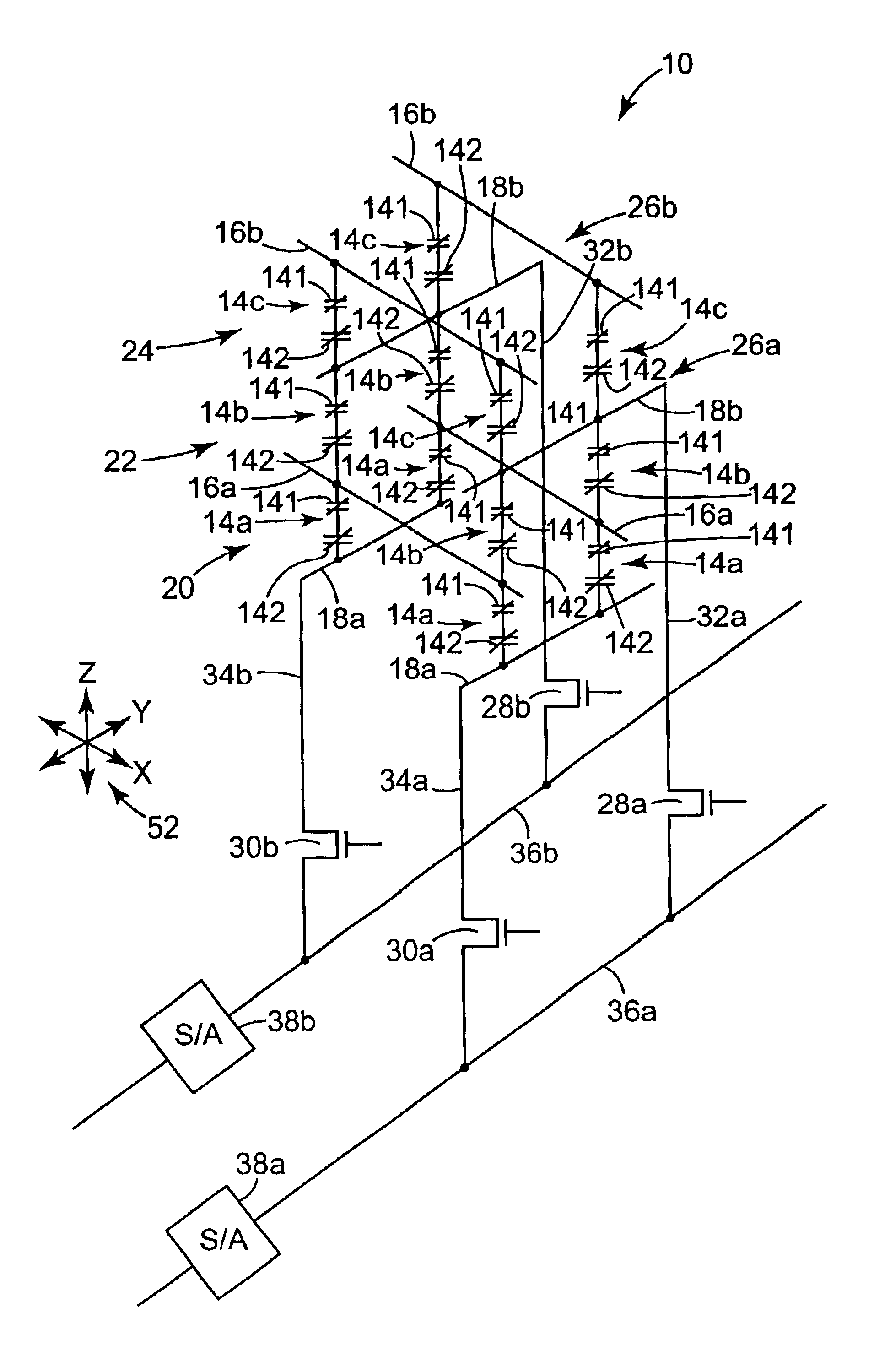
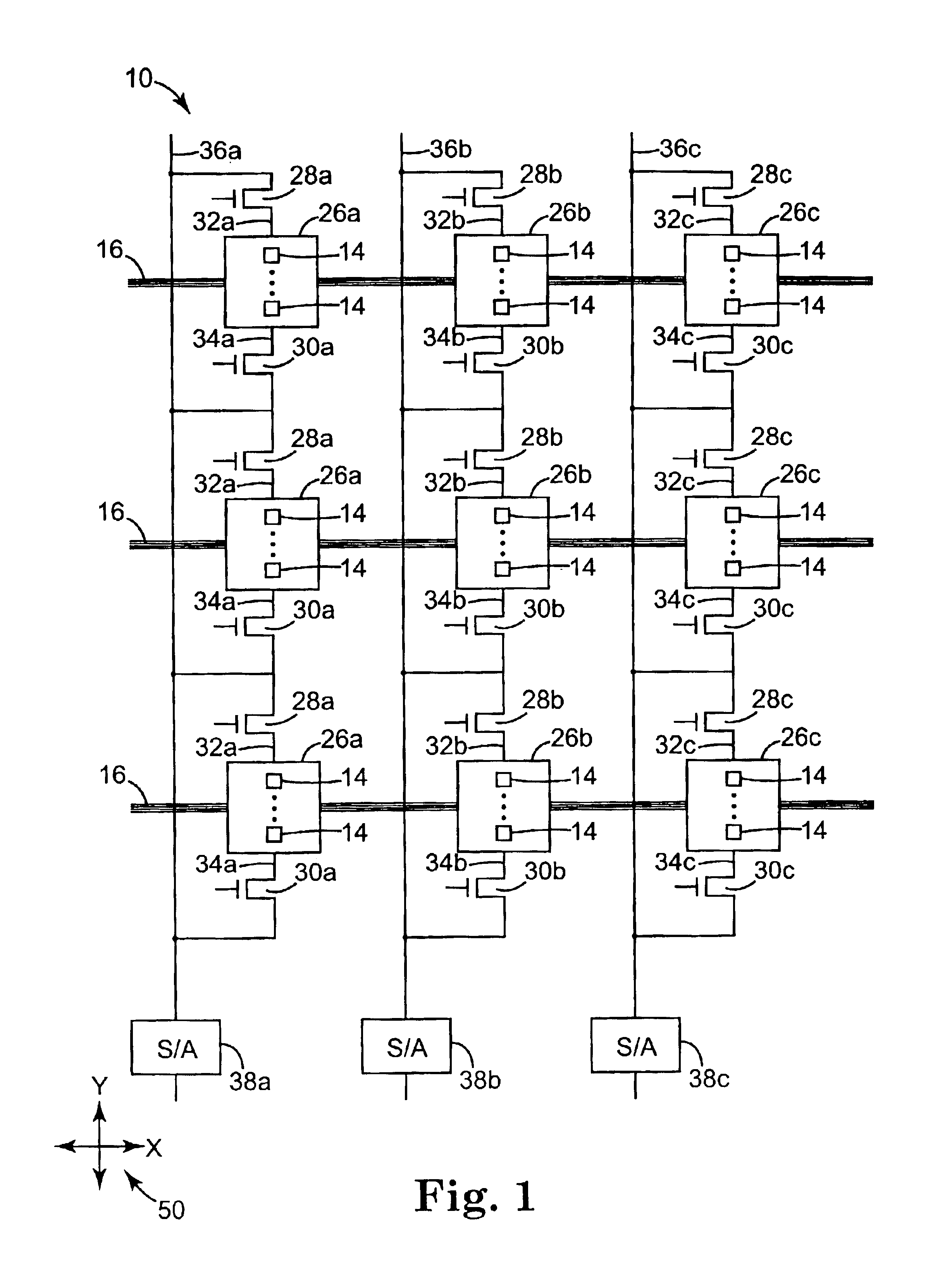
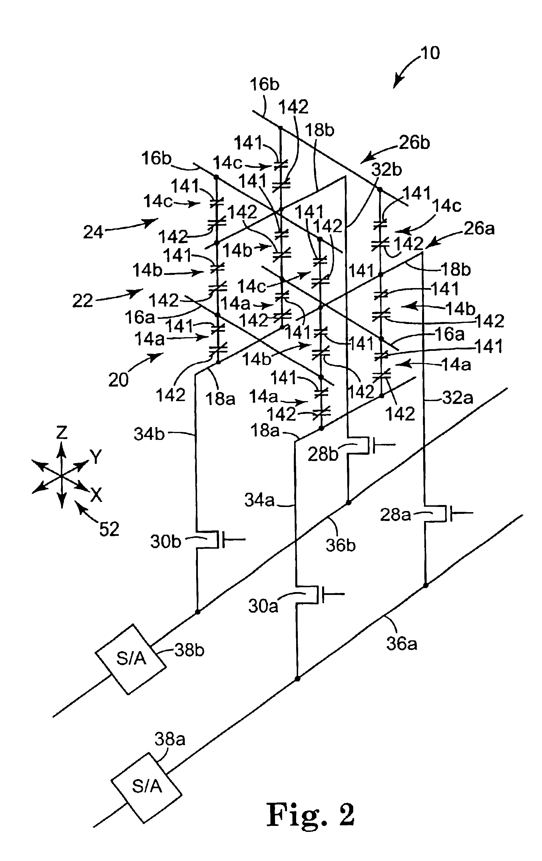
[0034]FIGS. 4A and 4B are cross section views illustrating a memory cell 14 used in a memory storage device according to the present invention. FIGS. 4A and 4B illustrate that each memory cell 14 is intersected and electrically coupled to a row line 16 and a column line segment 18. Memory cells in various embodiments are electrically coupled at a top side to column line segment 18 and at a bottom side to row lines 16, or at a bottom side to column line segments 18 and at a top side to row lines 16.

[0035]FIG. 4A illustrates a tunnel junction storage element 141 electrically coupled via electrode 41 to a tunnel junction control element 142. Control element 142 is electrically coupled to column line segments 18 via electrode 42. Storage element 141 is electrically coupled to row line 16 via electrode 40. Electrodes 40, 41 and 42 provide a low resistance contact to control element 142 and storage element 141 to minimize any unintended resistance to current flow through memory cell 14. I...

second embodiment

[0037]FIG. 5 is a cross section view illustrating a memory cell 14 used in a memory storage device according to the present invention. In the illustrated embodiment, a row line 16 is formed of a conductive thin-film such as aluminum and is deposited and etched to define row line 16. A planar dielectric layer 62 is formed over and above row line 16.

[0038]In the illustrated embodiment, after dielectric layer 62 has been formed, an etch step is completed to define an etched via region 64. The exposed row line 16 in the bottom of via region 64 is oxidized to form an oxide portion 60. In various embodiments, oxide portion 60 is formed through self-oxidation, is thermally grown, or is deposited. In one embodiment, oxide portion 60 has a thickness which is less than 100 Angstroms. In other embodiments, oxide portion 60 has a thickness which is less than 50 Angstroms. After oxide portion 60 is formed, a conductive thin-film metal layer 66 is deposited over dielectric layer 62 and a dielectr...

third embodiment

[0043]FIG. 6 is a cross section view illustrating a memory cell 14 used in a memory storage device according to the present invention. The construction of memory cell 14 is similar to the embodiment of FIG. 5 with the exception that the illustration in FIG. 6 includes a state-change layer 76. Many suitable phase-change materials can be used for a read / writeable (or write / erase / write) state-change layer in accordance with the present invention. In one embodiment, germanium telluride (GeTe) is used. GeTe can be reversibly changed from a semiconducting (amorphous) state to a metallic (crystalline) state by undergoing heating and cooling steps at a suitable rate. In one embodiment, the GeTe is doped so that it is p-type when in its semiconducting state. When GeTe is deposited over an n-type semiconductor layer, a large contrast is observed in the number of carriers swept across the junction when compared to GeTe in the metallic state. In various embodiments, when using GeTe or other sui...


PUM


Abstract

A memory storage device includes a first and second memory cell which each have a top end and a bottom end. A first and second first dimension conductor are substantially coplanar and parallel and extend in a first dimension. The first first dimension conductor intersects the bottom end of the first memory cell and the second first dimension conductor intersects the top end of the second memory cell. A first second dimension conductor extends in a second dimension and intersects the top end of the first memory cell and a second second dimension conductor extends in the second dimension and intersects the bottom end of the second memory cell. A first third dimension conductor which extends in a third dimension is positioned between the first and second memory cell to couple the first second dimension conductor to the second second dimension conductor.

Description

THE FIELD OF THE INVENTION[0001]The present invention relates to the field of integrated circuit memories. More particularly the present invention relates to a memory storage device and method for a three dimensional cross point memory array.BACKGROUND OF THE INVENTION[0002]As the demand for integrated circuits continues to rise, manufacturers labor to incorporate increasingly greater numbers of transistors onto each die. Integrated circuit memories often times have higher transistor densities than other types of circuits, and as a result, tend to push the leading edge of the technology envelope. The memories are typically organized into two dimensional arrays wherein each memory cell in the array is intersected by a row conductor and a column conductor. The two dimensional memory arrays are often times limited in memory cell density by the minimum line widths of the technology used to fabricate the array. As a result, improvements in the memory densities are achieved when the minim...

Claims


Application Information

Patent Timeline
Patent Type & Authority Patents(United States)
IPC IPC(8): G11C5/02H01L27/24H01L27/112H01L21/8246H01L27/105
CPCH01L27/24G11C5/025H10B63/00H01L27/10
Inventor VAN BROCKLIN, ANDREW L.FRICKE, PETER
Owner TAIWAN SEMICON MFG CO LTD
Why Eureka
Try Eureka