
Flash memory for improving write access time

a flash memory and write access technology, applied in the field of flash memory, can solve the problems of limited erase/rewrite life of flash memory cells, long write access time, and restrict the use of flash memory, so as to achieve the effect of effectively reducing write access time and avoiding unnecessary data verification

Active Publication Date: 2005-07-12
RENESAS ELECTRONICS CORP
View PDF7 Cites 43 Cited by
  • Summary
  • Abstract
  • Description
  • Claims
  • Application Information

AI Technical Summary

Benefits of technology

[0034]In detail, an object of the present invention is to provide a flash memory for reducing necessary time for pre-verification to achieve improved write access time.
[0036]This architecture avoids unnecessary data verification of an unupdated page(s), and thus effectively reduces write access time.

Problems solved by technology

One of the issues of flash memories is long write access time.
The long write access time of flash memories often restricts the use of the flash memories.
Another reason is the limited erase / rewrite life of flash memory cells.
Although pre-verification is inevitable for flash memories, the pre-verification undesirably increases write access time of the flash memories.
Executing repeated data verifications undesirably increases the write access time.

Method used


Image

  • Flash memory for improving write access time
  • Flash memory for improving write access time
  • Flash memory for improving write access time

Examples


Embodiment Construction

[0060]Preferred embodiments of the present invention are described below in detail with reference to the attached drawings.

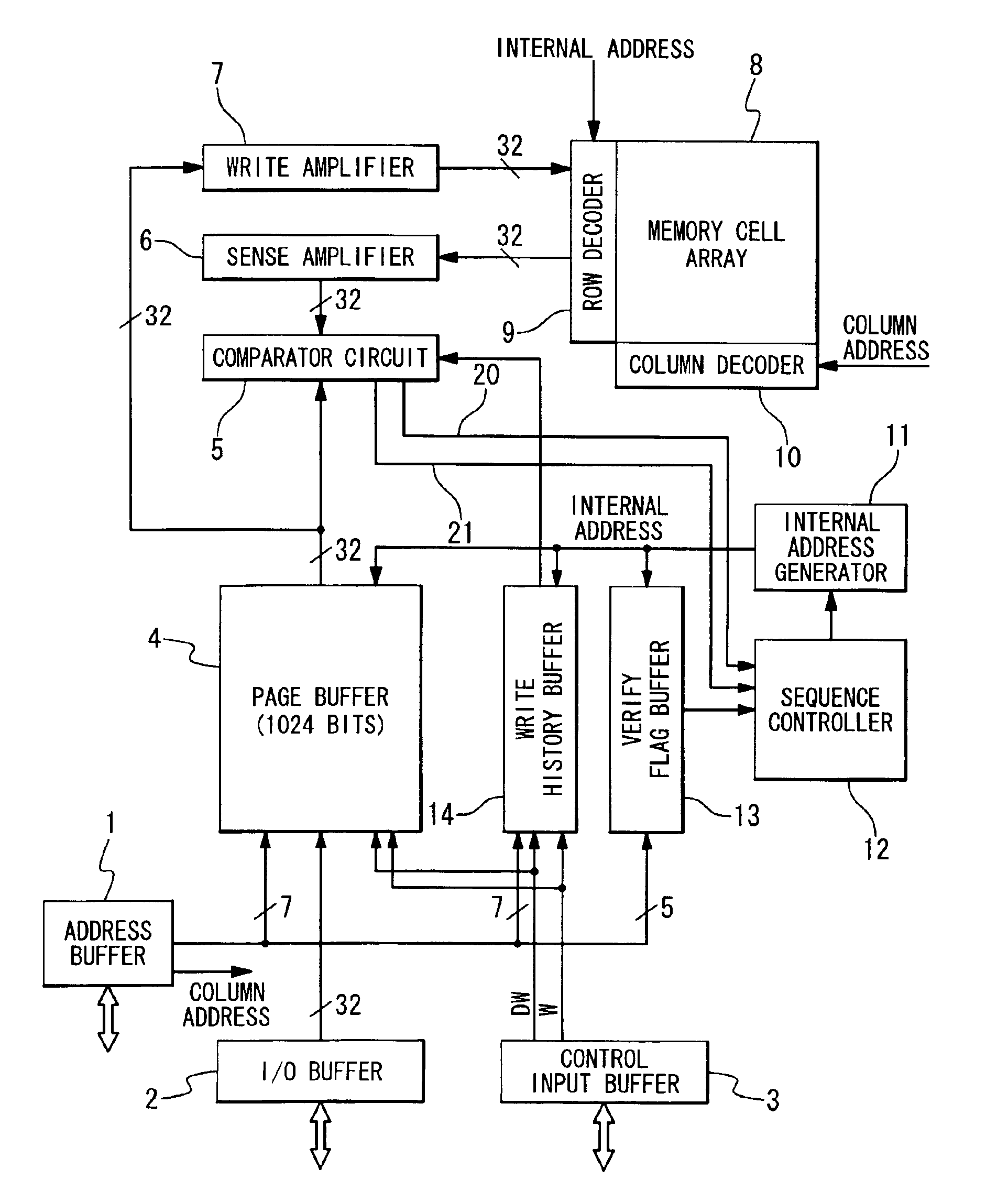
[0061]FIG. 4 is a block diagram of a flash memory in one embodiment according to the present invention. In FIG. 4, elements corresponding to those illustrated in FIG. 1 are denoted by the same numerals, and detailed explanations thereof are not given below to avoid repeated explanations.

[0062]The memory system structure of the flash memory in this embodiment is similar to that of the flash memory illustrated in FIG. 1, except for that the comparator circuit 85 and the sequence controller 92 are respectively replaced with a comparator circuit 5 and a sequence controller 12, and that a control input buffer 3, a verify flag buffer 13 and a write history flag buffer 14 are added to the flash memory.

[0063]The control input buffer 3 generates a pair of mode setting signals DW and W to allow the flash memory to be placed into a selected I / O mode in response to control ...


PUM


Abstract

A flash memory including a flash memory cell array, a page buffer, a comparator circuit, and a verify flag buffer. The flash memory cell array includes a plurality of blocks. The page buffer temporarily stores therein write data received from an external system. The page buffer includes pages. The comparator circuit executes pre-verification through comparing data stored in the page buffer with data stored in addressed one of the blocks. The verify flag buffer stores therein verify flags respectively associated with the pages. Each of the verify flags is switched in response to update of associated one of the pages. The comparator circuit executes pre-verification with respect to one of the pages, the one being associated with unswitched one of the verify flags, while skipping pre-verification with respect to another of the pages associated with the switched one of the verify flags.

Description

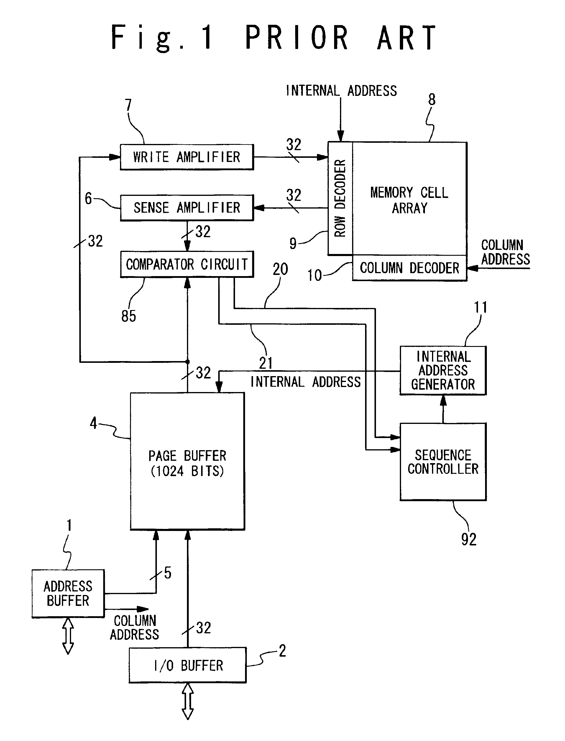
BACKGROUND OF THE INVENTION[0001]1. Field of the Invention[0002]The present invention is related, in general, to flash memories, in particular, to an improvement of write access time of flash memories.[0003]2. Description of the Related Art[0004]One of the issues of flash memories is long write access time. The long write access time of flash memories often restricts the use of the flash memories.[0005]In order to reduce write access time, build-in page buffer architecture has been developed. A typical build-in page buffer flash memory includes a static random access memory (SRAM), which has a fast read / write access time, as a page buffer. Write data is temporarily stored in the SRAM-based page buffer, and then transferred from the page buffer to the flash memory array.[0006]FIG. 1 is a block diagram of a typical build-in page buffer flash memory. The conventional flash memory is composed of an address buffer 1, an I / O buffer 2, a page buffer 4, a comparator circuit 85, a sense ampl...

Claims


Application Information

Patent Timeline
IPC IPC(8): G11C7/00G11C16/10G11C7/22G11C16/06G11C16/02G11C11/413
CPCG11C7/22G11C16/10G11C2216/14G11C2207/229G11C11/413
Inventor SATO, AKIRA
Owner RENESAS ELECTRONICS CORP
Learn More