LED package and the process making the same

a technology of led packaging and manufacturing process, which is applied in the field of photoelectric semiconductors, can solve the problems of poor thermal conductivity, small contact area between the die and one of the leads, and damage to the led package, and achieve the effect of durable and thermally conductive led packages

Inactive Publication Date: 2005-07-26
CREELED INC +1
View PDF2 Cites 57 Cited by
  • Summary
  • Abstract
  • Description
  • Claims
  • Application Information

AI Technical Summary

Benefits of technology

[0005]The primary objective of the present invention is to provide a process for fabricating LED packages, whereby a better thermally conductive and durable LED packages are made.

Problems solved by technology

Compared with other lighting devices, such as fluorescent lamps and incandescent lamps, the heat emitted by the LED package is low, but a certain amount of the heat, which is generated while the LED die glows by the electricity of from tens to hundreds of milliamperes, is a major factor resulted in the damage of the LED package.
As far as the foregoing prior art LED package is concerned, the die is encapsulated in the epoxy encapsulant, which thermal conductivity is poor, and the contact area between the die and one of the leads is small.
Besides, a protrudent portion of the leads out of the encapsulant is in the shape of a thin bar, so that the thermal conductivity of the above-mentioned conventional LED package is very poor and further improvement is required.

Method used


Image

  • LED package and the process making the same
  • LED package and the process making the same
  • LED package and the process making the same

Examples


Embodiment Construction

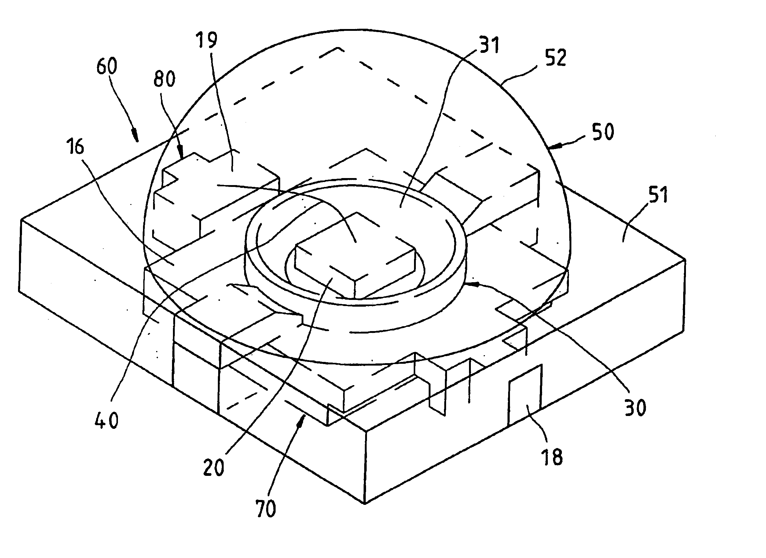
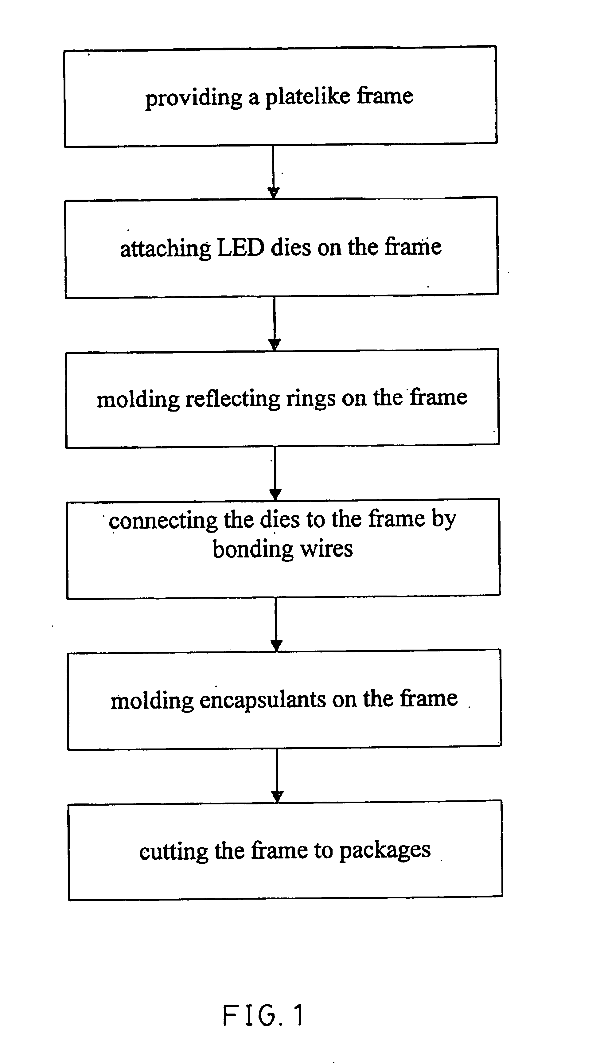
[0019]The preferred embodiment of the present invention is to provide a process for fabricating white LED packages. However, it is to be understood that this process can be applied to make any kind of the LED lamp packages. Referring to FIG. 1, a flow chart of a fabricative process of the present invention includes six steps of plate-like frame providing, die bonding, reflecting ring molding, wire bonding, encapsulant molding, and cutting. The details of the steps will be illustrated hereunder with the accompanying drawings.

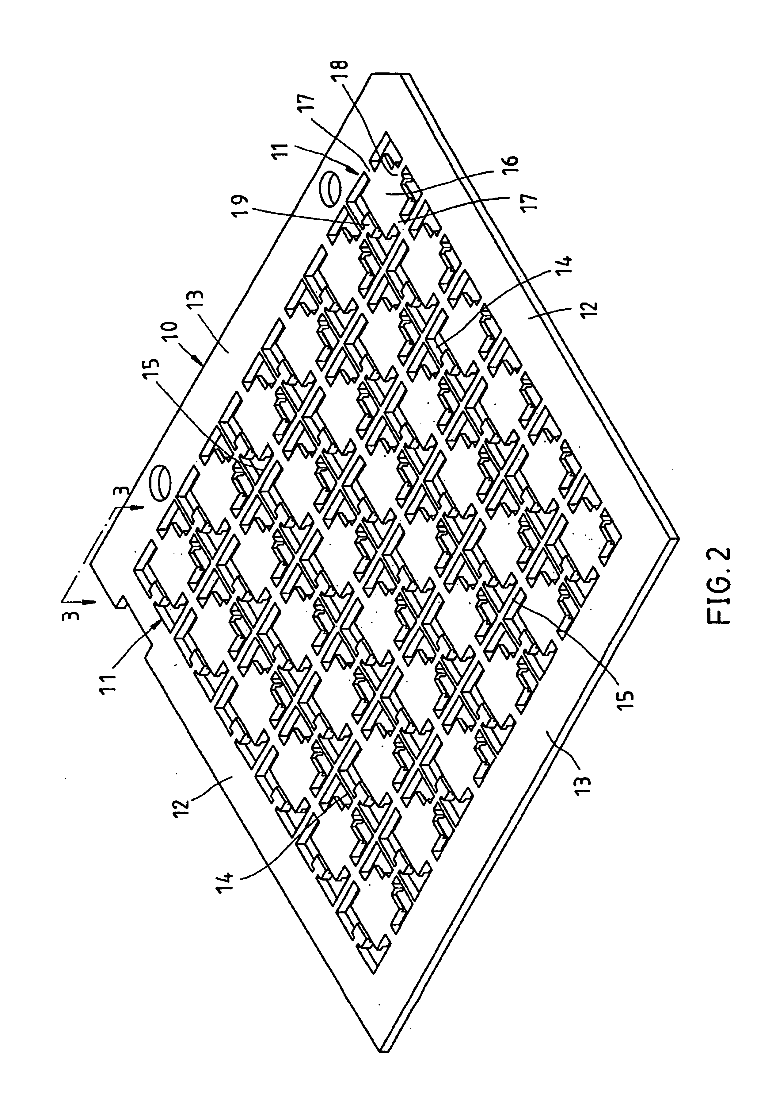
[0020]Referring to FIGS. 2-3, firstly, provide a plate-like frame 10, which is substantially rectangle and has a plurality of cells 11. The cells 11, each of which has a plurality of openings, are well positioned in an arrangement of matrix. Namely, the cells 11 are surrounded by left and right lateral sides, which are defined as two longitudinal lateral bars 12, and upper and lower sides, which are defined as two transversal lateral bars 13, wherein each of the ...


PUM


Abstract

Light emitting diode (LED) packages are made by first providing a platelike frame having a plurality of cells, each of which is composed of a main plate and a separate arm. Secondly, an LED die and a reflecting ring are respectively mounted on top of each main plate such that the die is located at a center of the reflecting ring. Then a conductive wire is connected between the top surface of the die and a top surface of the separate arm by wire bonding. A domed transparent encapsulant is then molded on each of the cells. The encapsulant encapsulates the die, the reflecting ring and the conductive wire and covers the main plate and the separate arm, and fills a space between the main plate and the separate arm to remain their spaced apart. Finally, the frame is cut according to the size of each cell to obtain the LED packages.

Description

[0001]This is a division of parent application Ser. No. 10 / 263,805, filed Oct. 4, 2002, now U.S. Pat. No. 6,770,498.FIELD OF THE INVENTION[0002]The present invention relates generally to photoelectric semiconductor, and more particularly to a process for fabricating a light emitting diode (LED) package and the structure of the LED package.BACKGROUND OF THE INVENTION[0003]A conventional lamp-typed LED package is made by the following process. Firstly, provide a frame made of an electrically conductive metal. The frame has a numbers of pairs of leads arranged parallel and interconnected with each others through a cross bar. Each pair of leads is served as a positive pole and a negative pole of one LED package. On one of the poles, generally the negative pole, a bowl-shaped recess defining a reflecting surface for reflecting light is formed. Next, an LED die is attached on a bottom of the bowl-shaped recess of each negative pole by an electrically conductive adhesive, e.g. silver adhes...

Claims


Application Information

Patent Timeline
Patent Type & Authority Patents(United States)
IPC IPC(8): H01L33/00H01L33/48H01L33/60H01L33/62
CPCH01L33/486H01L33/62H01L24/97H01L33/60H01L2224/48091H01L2224/48247H01L2924/01079H01L2924/00014H01L2224/45144H01L2924/00H01L2924/12041H01L33/642
Inventor HSU, CHENG-HSIANG
Owner CREELED INC
Why Eureka
Try Eureka