Interdigitated capacitor and method of manufacturing thereof

a technology of interdigitated capacitors and capacitors, which is applied in capacitors, radiation controlled devices, semiconductor devices, etc., can solve the problems of affecting the size of interdigitated capacitors, affecting the performance of interdigitated capacitors, and poor conductivity of healing electrodes,

Inactive Publication Date: 2005-08-09
BELL SEMICON LLC
View PDF7 Cites 29 Cited by
  • Summary
  • Abstract
  • Description
  • Claims
  • Application Information

AI Technical Summary

Problems solved by technology

However, since the capacitance of such capacitors depends somewhat on the surface area of their electrodes, decreasing the size of these capacitors is hampered by the need for a high surface area.
Unfortunately, in addition to the increased risk of layer defects, as capacitor films become thinner they operate closer to the breakdown point of the layer.
However, those skilled in the art understand that healing electrodes have relatively poor conductivity, making electrolytic capacitors a poor choice for high frequency (e.g., >1 Mhz) applications.
Moreover, even if capacitor layer thickness were further reduced, without the adverse consequences discussed above, forming an increased number of layers, for example in an MLCC, results in increased manufacturing steps, which translates into increased manufacturing costs.
With the already high cost of semiconductor manufacturing, as well as a market already filled with intense competition, semiconductor manufacturers must make every effort to stream-line the manufacturing process rather than increase the cost.

Method used


Image

  • Interdigitated capacitor and method of manufacturing thereof
  • Interdigitated capacitor and method of manufacturing thereof
  • Interdigitated capacitor and method of manufacturing thereof

Examples


Embodiment Construction

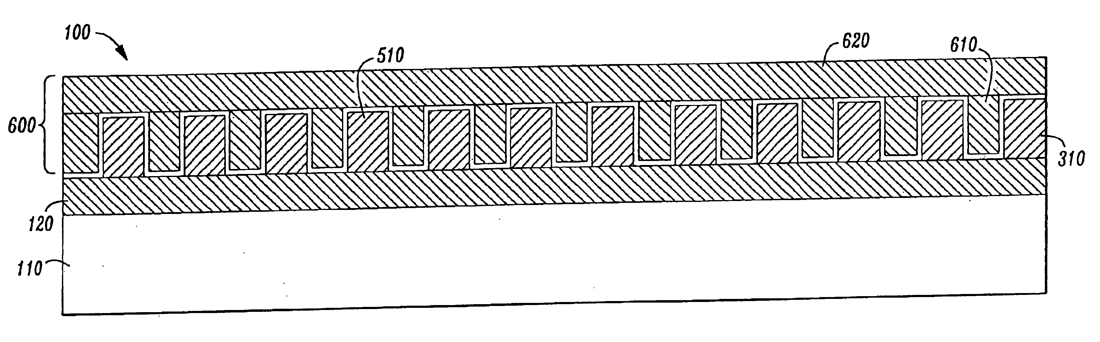
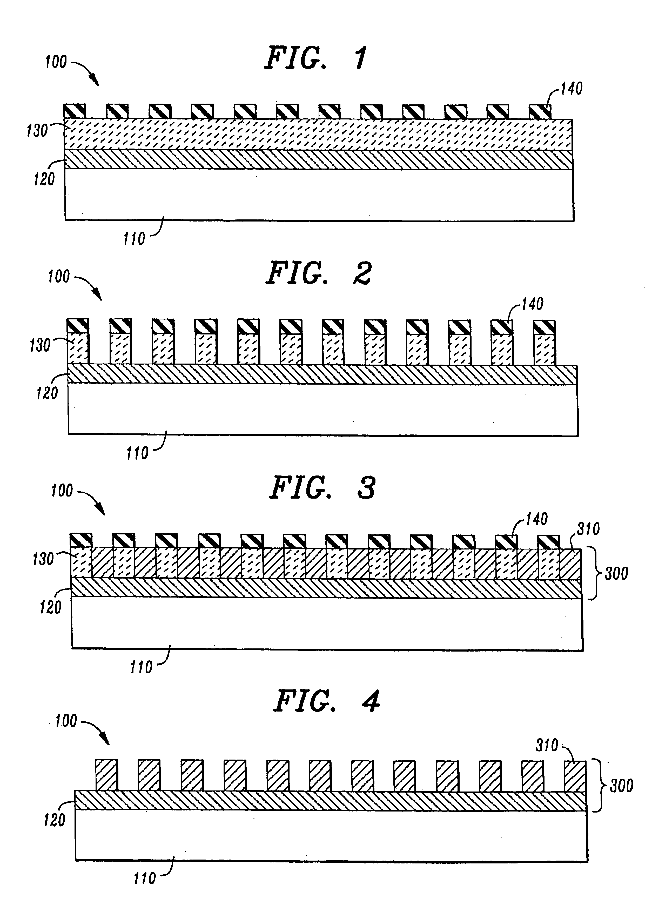
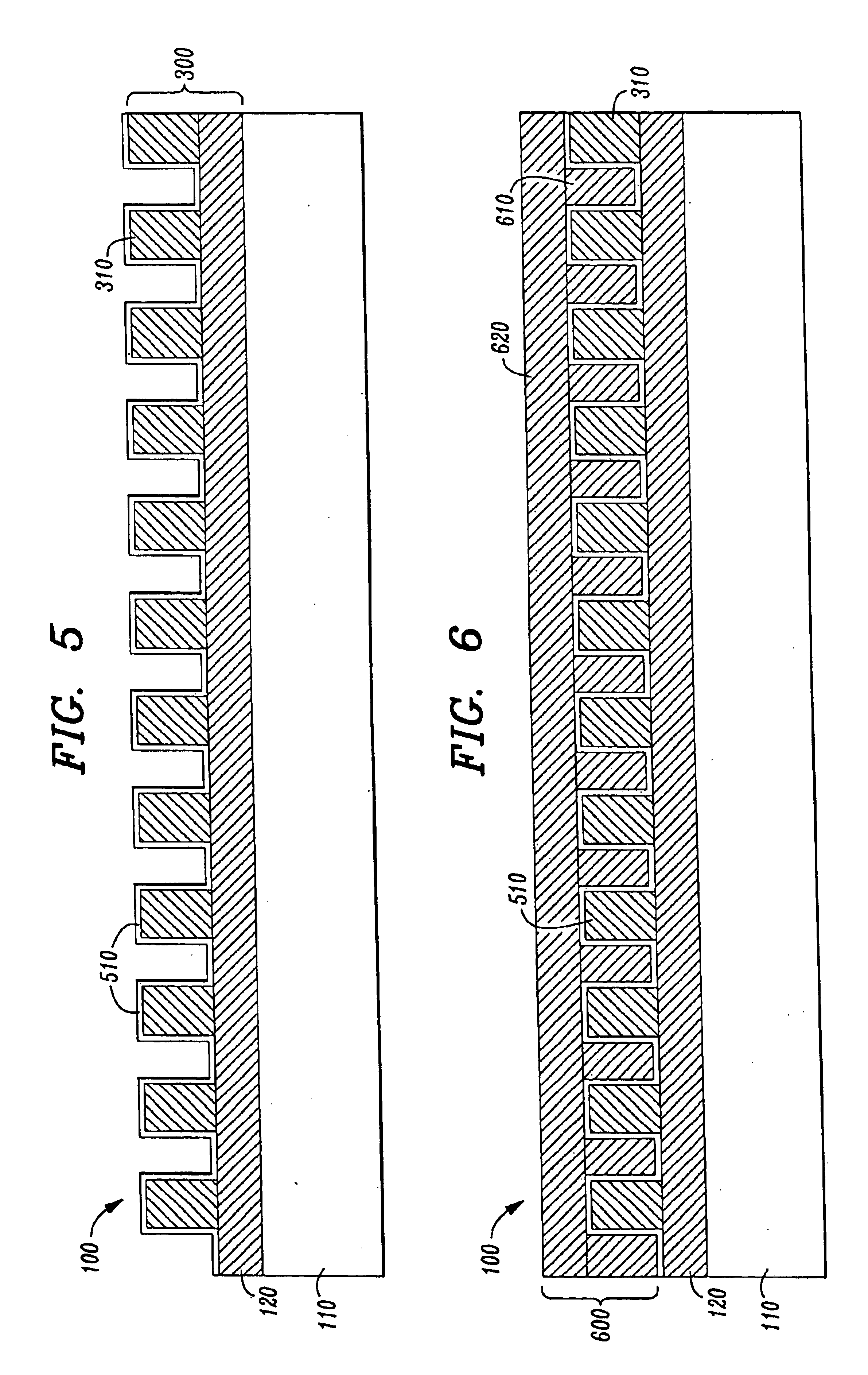
[0021]Referring initially to FIG. 1, illustrated is a sectional view of an initial device 100 from which an interdigitated capacitor as provided by the present invention may be formed. The device 100 is formed on a semiconductor substrate 110, which may be comprised of silicon. Deposited on top of the substrate 110 is a first conductive layer 120. In an advantageous embodiment of the present invention, the first conductive layer 120 may be copper. Of course, the first conductive layer 120 may be comprised of any suitable conductor, and the present invention is not limited to any particular conductive material.

[0022]On top of the first conductive layer 120, a sacrificial layer 130 is deposited. In one embodiment the sacrificial layer 130 may be silicon dioxide (SiO2), however any suitable material may be used. A mask 140, such as a photoresist layer, is then deposited atop the sacrificial layer 130 and patterned, preferably using conventional photolithographic techniques. The pattern...


PUM


Abstract

The present invention provides a method of manufacturing an interdigitated semiconductor device. In one embodiment, the method comprises simultaneously forming first electrodes adjacent each other on a substrate, forming a dielectric layer between the first electrodes, and creating a second electrode between the first electrodes, the second electrode contacting the dielectric layer between the first electrodes to thereby form adjacent interdigitated electrodes. An interdigitated capacitor and a method of manufacturing an integrated circuit having an interdigitated capacitor are also disclosed.

Description

[0001]This Application is a Divisional of prior application Ser. No. 09 / 929,188 filed on Aug. 14, 2001, now U.S. Pat. No. 6,740,922, to Christopher D. W. Jones, et al. The above-listed Application is commonly assigned with the present invention and is incorporated herein by reference as if reproduced herein in its entirety under Rule 1.53(b).TECHNICAL FIELD OF THE INVENTIONBackground of the Invention[0002]As is well known, various semiconductor devices and structures are fabricated on semiconductor wafers in order to form operative integrated circuits (ICs). These various semiconductor devices and structures allow fast, reliable and inexpensive ICs to be manufactured for today's competitive computer and telecommunication markets. To keep such ICs inexpensive, the semiconductor manufacturing industry continually strives to economize each step of the IC fabrication process to the greatest extent, while maintaining the highest degree of quality and functionality as possible.[0003]Integ...

Claims


Application Information

Patent Timeline
Patent Type & Authority Patents(United States)
IPC IPC(8): H01L21/02H01L27/08
CPCH01L27/0805H01L28/91
Inventor JONES, CHRISTOPHER D. W.MURPHY, DONALD W.WONG, YIU-HUEN
Owner BELL SEMICON LLC
Why Eureka
Try Eureka