Magnetic random access memory

Inactive Publication Date: 2005-08-09
KK TOSHIBA
View PDF10 Cites 24 Cited by
  • Summary
  • Abstract
  • Description
  • Claims
  • Application Information

AI Technical Summary

Benefits of technology

[0048]FIG. 4 is a graph showing the effect of increasing

Problems solved by technology

In the memory using the MTJ element, the write current value is higher than an ideal value (8 to 10 mA), and the write current value greatly varies between bit lines, generating a write error.
However, ensuring thermal disturbance resistance limits a decrease in the thickness of the recording layer of the MTJ element.
As a result, the magnetic field H necessary to reverse the magnetization direction of the recording layer cannot be generated.
However, the write current va

Method used


Image

  • Magnetic random access memory
  • Magnetic random access memory
  • Magnetic random access memory

Examples


first embodiment

2. First Embodiment

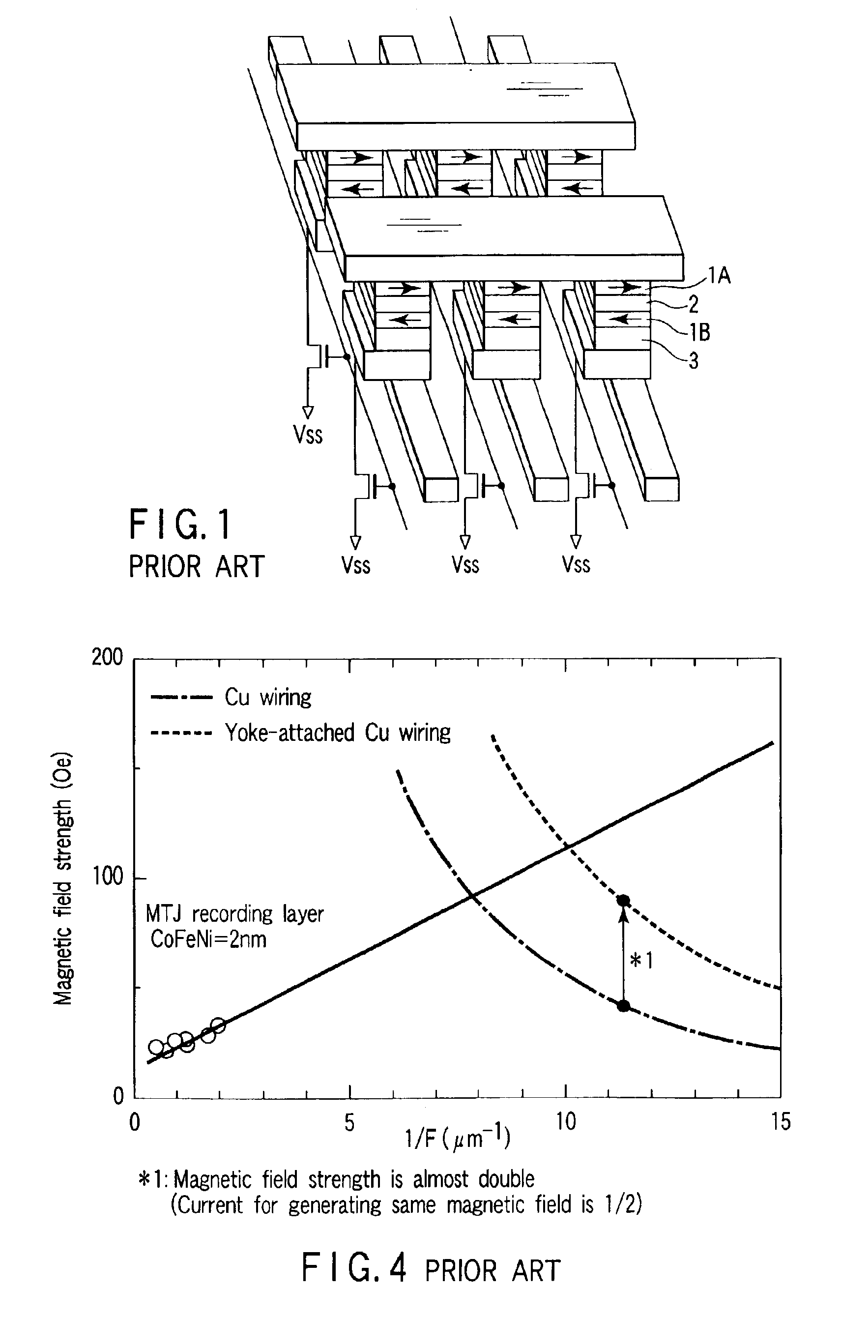
[0082]FIG. 6 shows the device structure of the main part of a magnetic random access memory according to the first embodiment of the present invention. FIG. 7 is a perspective view three-dimensionally showing the structure of FIG. 6.

[0083]A write line 4 runs along the X-axis, and a write line 5 runs along the Y-axis. The write lines 4 and 5 are made of, e.g., Cu. An MTJ element 6 is arranged at the intersection of the two write lines 4 and 5 crossing each other. The MTJ element 6 has a rectangular shape which is long along the X-axis and short along the Y-axis. In this case, the easy axis of magnetization of the MTJ element 6 is the X-axis.

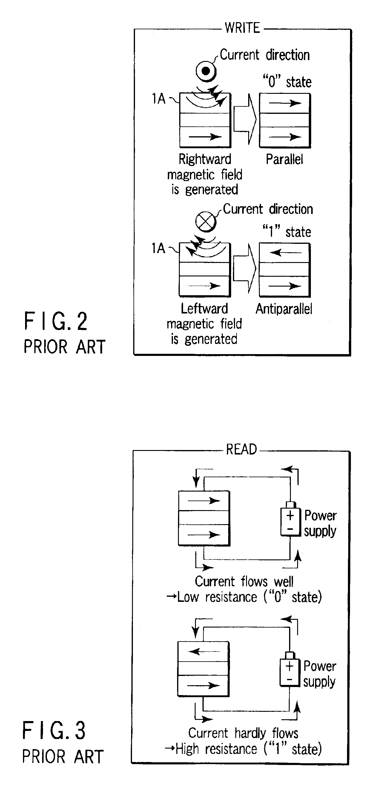
[0084]The MTJ element 6 is made up of, e.g., a recording layer (magnetic layer) 1A, fixed layer (magnetic layer) 1B, tunneling barrier layer 2, and antiferromagnetic layer 3. The antiferromagnetic layer 3 of the MTJ element 6 is arranged on the write line 4 side. The antiferromagnetic layer 3 is made of, e.g., PtMn or CoFe. The ...

second embodiment

3. Second Embodiment

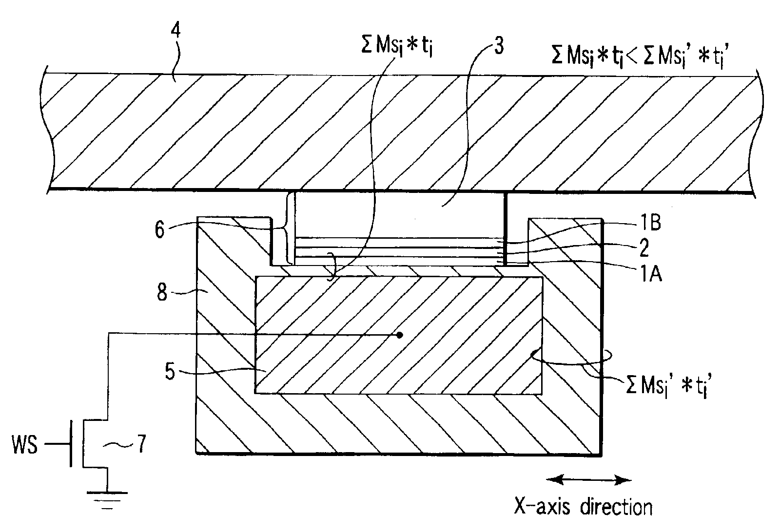
[0091]FIG. 8 shows the device structure of the main part of a magnetic random access memory according to the second embodiment of the present invention.

[0092]The device structure of the second embodiment is different from that of the first embodiment in that the X-axis (easy axis of magnetization) end of an MTJ element 6 is in contact with a yoke material 8. In this case, the recording layer of the MTJ element 6 is exchange-coupled to the yoke material 8 on the lower and side surfaces. The remaining structure is the same as that of the first embodiment.

[0093]Also in the second embodiment, the total magnetic volume ΣMsi×ti of the recording layer of the MTJ element 6 and a portion of the yoke material 8 that is exchange-coupled to the recording layer is set smaller than the magnetic volume ΣMsi′×ti′ of the remaining portion of the yoke material 8 that covers a write line 5.

third embodiment

4. Third Embodiment

[0094]FIG. 9 shows the device structure of the main part of a magnetic random access memory according to the third embodiment of the present invention.

[0095]The device structure of the third embodiment is different from that of the second embodiment in that no yoke material exists immediately below an MTJ element 6, i.e., the lower surface of the MTJ element 6 is in contact with the upper surface of a write line 5 without the mediacy of any yoke material.

[0096]The MTJ element 6 is in contact with a yoke material 8 on only the X-axis (easy axis of magnetization) end. In this case, the recording layer of the MTJ element 6 is exchange-coupled to the yoke material 8 on the side surface. The remaining structure is the same as that of the second embodiment.

[0097]Also in the third embodiment, the total magnetic volume ΣMsi×ti of the recording layer of the MTJ element 6 and a portion of the yoke material 8 that is exchange-coupled to the recording layer is set smaller tha...


PUM


Abstract

A write line is covered with a yoke material. The recording layer of an MTJ element is exchange-coupled to the yoke material. The total magnetic volume ΣMsi×ti of the recording layer of the MTJ element and a portion of the yoke material that is exchange-coupled to the recording layer is smaller than the magnetic volume ΣMsi′×ti′ of the remaining portion of the yoke material that covers the write line.

Description

CROSS-REFERENCE TO RELATED APPLICATIONS[0001]This application is based upon and claims the benefit of priority from the prior Japanese Patent Application No. 2002-340043, filed Nov. 22, 2002, the entire contents of which are incorporated herein by reference.BACKGROUND OF THE INVENTION[0002]1. Field of the Invention[0003]The present invention relates to a magnetic random access memory (MRAM) with high write reproducibility and high write efficiency.[0004]2. Description of the Related Art[0005]Magnetic random access memories have been studied and developed as ultimate nonvolatile high-speed, large-capacity memories.[0006]GMR (Giant Mangeto-Resistance) elements or MTJ (Magnetic Tunneling Resistance) elements are known as memory cells of magnetic random access memories. For data read, a memory using an MTJ element can ensure a larger signal amount than a memory using a GMR element. At present, magnetic random access memories using MTJ elements have enthusiastically been studied and deve...

Claims


Application Information

Patent Timeline
IPC IPC(8): G11C11/16G11C11/02G11C11/15H01L21/8246H01L27/105H01L43/08
CPCG11C11/16G11C11/15
Inventor YODA, HIROAKIASAO, YOSHIAKIUEDA, TOMOMASAMIYAMOTO, JUNICHIKISHI, TATSUYAAMANO, MINORUKAJIYAMA, TAKESHIAIKAWA, HISANORI
Owner KK TOSHIBA
Why Eureka
Try Eureka