Magnetically shielded conductor

a conductor and magnet shielding technology, applied in the field of magnet shielding conductors, can solve the problems of large current flows, high current flows, and often induced currents in implanted conductors

Inactive Publication Date: 2005-08-16
BIOPHAN TECH
View PDF6 Cites 90 Cited by
  • Summary
  • Abstract
  • Description
  • Claims
  • Application Information

AI Technical Summary

Problems solved by technology

When a patient with one of these implanted devices is subjected to high intensity magnetic fields, currents are often induced in the implanted conductors.
The large current flows so induced often create substantial amounts of heat.
Because living organisms can generally only survive within a relatively narrow range of temperatures, these large current flows are dangerous.
Furthermore, implantable devices, such as implantable pulse generators (IPGs) and cardioverter defibrillator / pacemaker (CDPs), are sensitive to a variety of forms of electromagnetic interference (EMI).
Because the sensing systems and conductive elements of these implantable devices are responsive to changes in local electromagnetic fields, they are vulnerable to external sources of severe electromagnetic noise, and in particular to electromagnetic fields emitted during magnetic resonance imaging (MRI) procedures.
One additional problem with implanted conductors is that, when they are conducting electricity and are simultaneously subjected to large magnetic fields, a Lorentz force is created which often causes the conductor to move.
This movement may damage body tissue.
Although the device of this patent does provide magnetic shielding, it still creates heat when it interacts with strong magnetic fields.

Method used


Image

  • Magnetically shielded conductor
  • Magnetically shielded conductor
  • Magnetically shielded conductor

Examples


Embodiment Construction

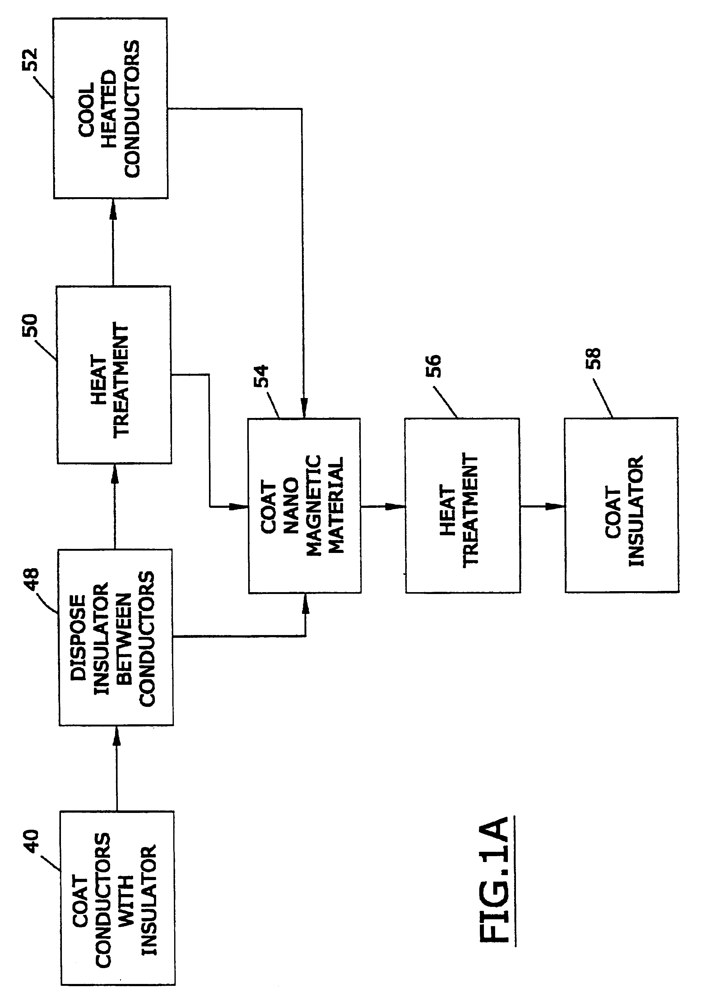
[0031]This specification is divided into two separate sections. In the first section of the case, a coated conductor assembly is described. In the second section of the case, a multiplicity of devices comprised of coated elements are described.

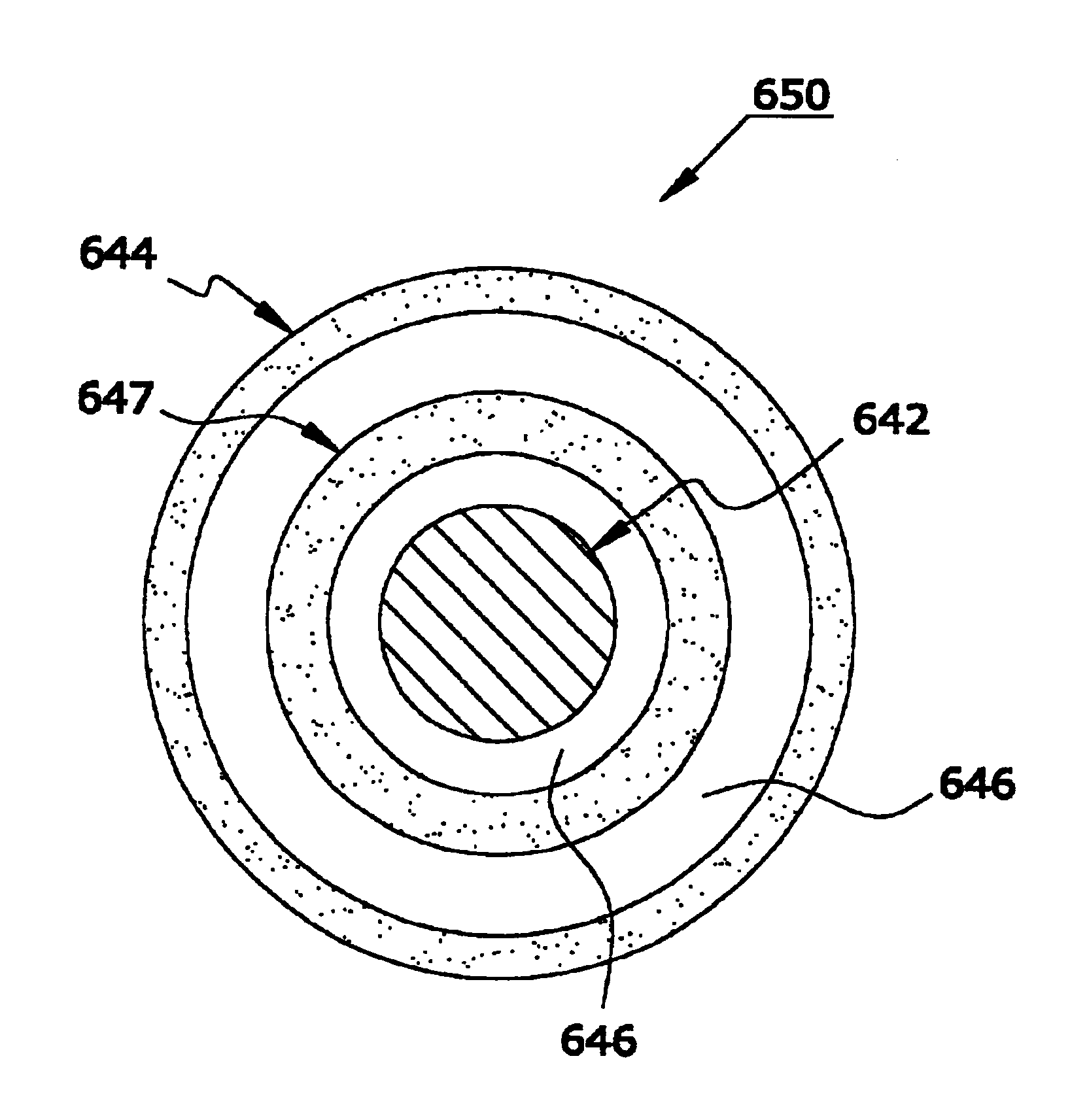
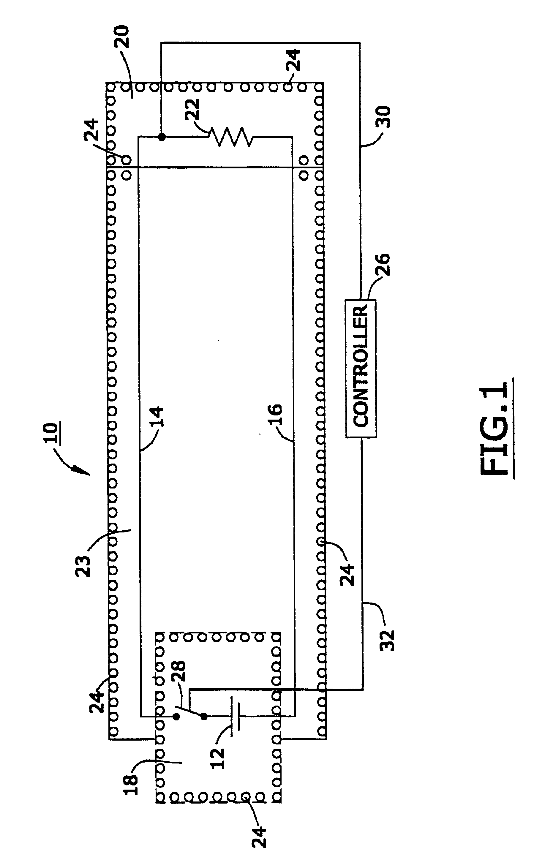
[0032]FIG. 1 is a schematic sectional view of one preferred device 10 that, in one embodiment, is implanted in a living organism. Referring to FIG. 1, it will be seen that device 10 is comprised of a power source 12, a first conductor 14, a second conductor 16, a first insulative shield 18 disposed about power source 12, a second insulative shield 20 disposed about a load 22, a third insulative shield 23 disposed about a first conductor 14, and a second conductor 16, and a multiplicity of nanomagentic particles 24 disposed on said first insulative shield, said second insulative shield, and said third insulative shield.

[0033]In the embodiment depicted in FIG. 1, the power source 12 is a battery 12 that is operatively connected to a controller 2...


PUM

PropertyMeasurementUnit
particle sizeaaaaaaaaaa
thicknessaaaaaaaaaa
particle size distributionaaaaaaaaaa

Abstract

A conductor assembly that contains a flexible conductor and a layer of nanomagnetic material coated onto the conductor. The layer of nanomagnetic material has a tensile modulus of elasticity of at least about 15×106 pounds per square inch, an average particle size of less than 100 nanometers, a saturation magnetization of from about 200 to about 26,000 Gauss, and a thickness of less than about 2 microns.

Description

CROSS-REFERENCE TO RELATED PATENT APPLICATION[0001]This patent application is a continuation-in-part of applicants' patent application U.S. Ser. No. 10 / 054,407, filed on Jan. 22, 2002, now U.S. Pat. No. 6,506,972.FIELD OF THE INVENTION[0002]A conductor assembly comprised of a conductor assembly disposed within an insulating sheath, wherein the sheath is coated with nanomagnetic material.BACKGROUND OF THE INVENTION[0003]Many implanted medical devices that are powered by electrical energy have been developed. Most of these devices comprise a power source, one or more conductors, and a load.[0004]When a patient with one of these implanted devices is subjected to high intensity magnetic fields, currents are often induced in the implanted conductors. The large current flows so induced often create substantial amounts of heat. Because living organisms can generally only survive within a relatively narrow range of temperatures, these large current flows are dangerous.[0005]Furthermore, imp...

Claims


Application Information

Patent Timeline
Patent Type & Authority Patents(United States)
IPC IPC(8): A61N1/16H01B7/04H01B11/10H01F10/00H01F10/32
CPCB82Y25/00H01B11/10H01B11/1083H01F10/007H01F10/324A61N1/3718H01F1/0063A61N1/086
Inventor HELFER, JEFFREY L.WANG, XINGWU
Owner BIOPHAN TECH
Why Eureka
Try Eureka