Prober

a technology of probes and probes, applied in the field of probes, can solve the problems of lowering throughput, surface damage, and inability to favorably measure electric characteristics, and achieve the effects of high throughput, good measurement, and mechanical vibration

Inactive Publication Date: 2005-08-23
TOKYO ELECTRON LTD +1
View PDF9 Cites 62 Cited by
  • Summary
  • Abstract
  • Description
  • Claims
  • Application Information

AI Technical Summary

Benefits of technology

[0014]According to the present invention, the object of the invention may be achieved. That is, the mechanical vibration may be earlier reduced, good measurement may be conducted with high throughput, and generation of damage of the electrode pads by the vibration may be inhibited.

Problems solved by technology

However, when the wafer-stage is stopped after it is moved, mechanical vibrations caused by moving and stopping the wafer-stage may remain in respective components of the probe apparatus.
Because of the mechanical vibrations, the contact state between a group of electrode pads and the group of probe needles may become unstable, which may make it impossible to favorably measure the electric characteristic.
However, if such a delay time becomes long, throughput may be lowered.
In addition, if a vibration is given to a group of electrode pads of semiconductor devices and the group of probe needles when they come in contact with each other, the surfaces of electrode pads may be scratched by the probe needles in an undesired manner so that the surfaces may be damaged.
Furthermore, if the above mechanical vibration is transmitted to a camera or the like used for a positioning operation, focusing thereof may not be achieved.
Even if the focusing is achieved, the image of the camera may hobble and thus the positioning operation may not be achieved.
Thus, anyway, the positioning operation has to be waited until the vibration is attenuated, which may badly affect the throughput.
Therefore, the problems of the above mechanical vibration tend to be especially significant.

Method used


Image

  • Prober
  • Prober
  • Prober

Examples


Embodiment Construction

[0028]Hereinafter, embodiments of the present invention are explained with reference to attached drawings.

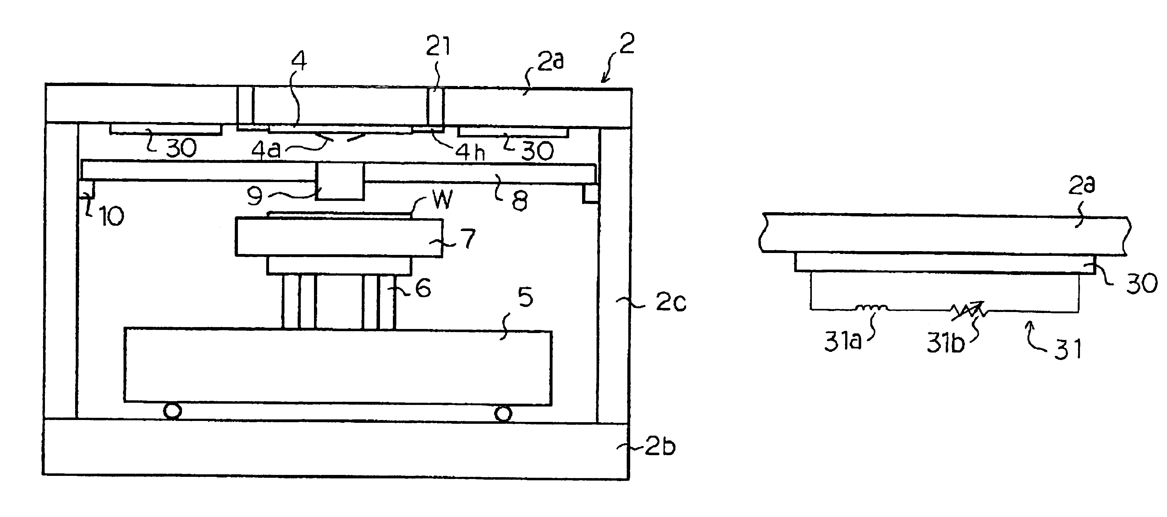
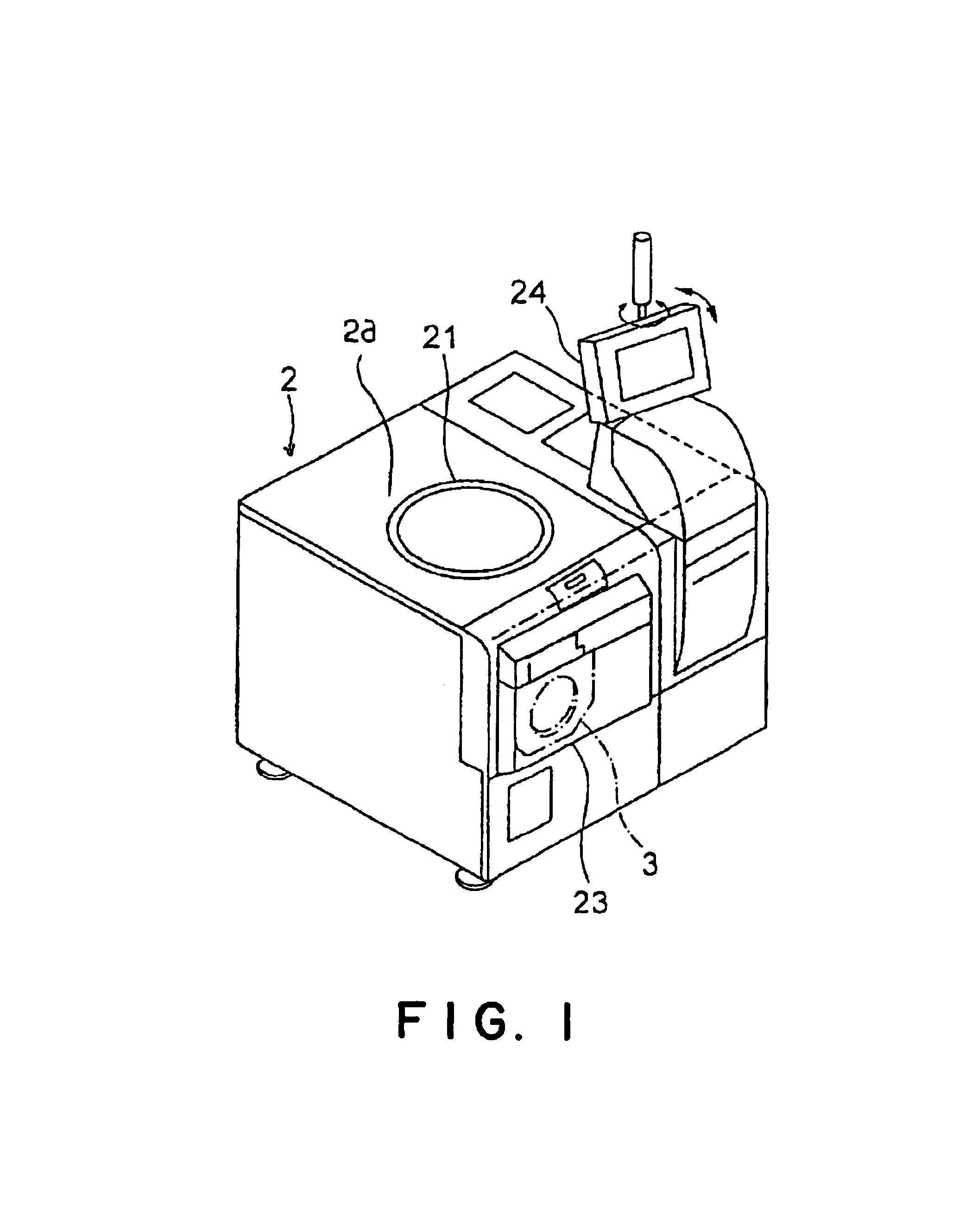
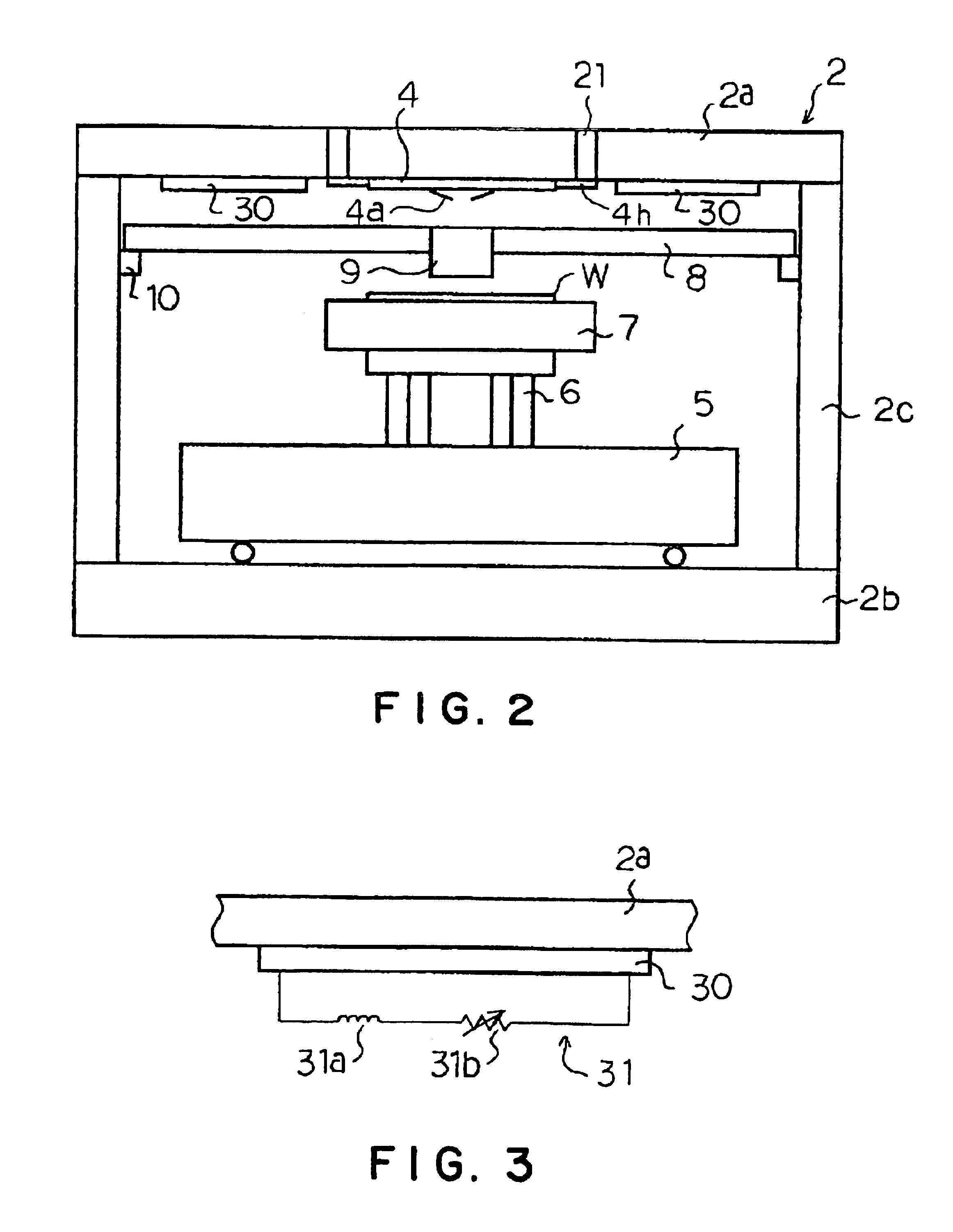
[0029]FIGS. 1 and 2 show a structure of a probe apparatus according to an embodiment of the present invention. FIG. 1 is a perspective view of the total probe apparatus, and FIG. 2 is a sectional view of main parts of the probe apparatus.

[0030]As shown in FIGS. 1 and 2, the probe apparatus of the embodiment includes a housing 2 as an outer container. An upper surface of the housing 2 serves as a head plate 2a. The head plate 2a is provided with an insert ring 21. A probe-card holding mechanism 4h is provided at the insert ring 21. A probe card 4 is detachably held by means of the probe-card holding mechanism 4h.

[0031]In the housing 2, a wafer cassette (not shown) containing semiconductor wafers, a conveying mechanism for conveying the semiconductor wafers between a wafer-stage 7 and the wafer cassette, and so on are contained.

[0032]In addition, in FIG. 1, the reference number 3...


PUM


Abstract

This invention is a probe apparatus including: a stage onto which a substrate to be processed is placed, a semiconductor device having a plurality of groups of electrode pads being formed on the substrate to be processed; a probe-card holding mechanism that holds a probe card provided with a group of probe needles corresponding to each group of electrode pads; and a driving mechanism that moves the stage and causes the group of probe needles to successively come in contact with the respective groups of electrode pads. A converting device that converts mechanical vibration energy generated in components of the probe apparatus into electrical energy, and an electrical circuit that discreates an electrical current based on the electric energy converted by the converting device are further provided.

Description

FIELD OF THE INVENTION[0001]This invention relates to a probe apparatus that carries out an electric inspection to a semiconductor device formed on a substrate to be measured such as a semiconductor wafer, by causing a probe stylus of a probe card to come in contact with the semiconductor device.BACKGROUND ART[0002]Conventionally, for example in a field of manufacturing semiconductor units, with respect to many semiconductor devices formed on a semiconductor wafer, before the semiconductor wafer is cut and divided, an electric characteristic of each of the many semiconductor devices is measured to examine whether it is defective or not. A probe apparatus is used for the examination.[0003]A wafer-stage that can hold a semiconductor wafer is provided in the probe apparatus. The wafer-stage is provided with a driving mechanism, which includes an X-Y drive mechanism such as an X-Y table and a Z-axis drive mechanism or the like. By means of the driving mechanism, a semiconductor wafer he...

Claims


Application Information

Patent Timeline
Patent Type & Authority Patents(United States)
IPC IPC(8): G01R31/28G01R31/26F16F15/02G01R1/06H01L21/66
CPCG01R31/2887G01R31/2851H01L22/00
Inventor KOBAYASHI, MASAHITOYOSHIOKA, HARUHIKOFUJITA, TAKAFUMI
Owner TOKYO ELECTRON LTD
Why Eureka
Try Eureka