

Ion microscope
a technology of ion microscope and gas field ion source, which is applied in the direction of material analysis using wave/particle radiation, instruments, nuclear engineering, etc., can solve the problems of gas supplied into the ionizing chamber, no description of the cooling mechanism of the charged particle source, and the high-temperature vacuum sample chamber wall, etc., to improve the brightness of the ion source, improve the focusing performance of the ion beam, and reduce the mechanical vibration of the refrigerator
- Summary
- Abstract
- Description
- Claims
- Application Information
AI Technical Summary
Benefits of technology
Problems solved by technology
Method used
Image

Examples
embodiment 1
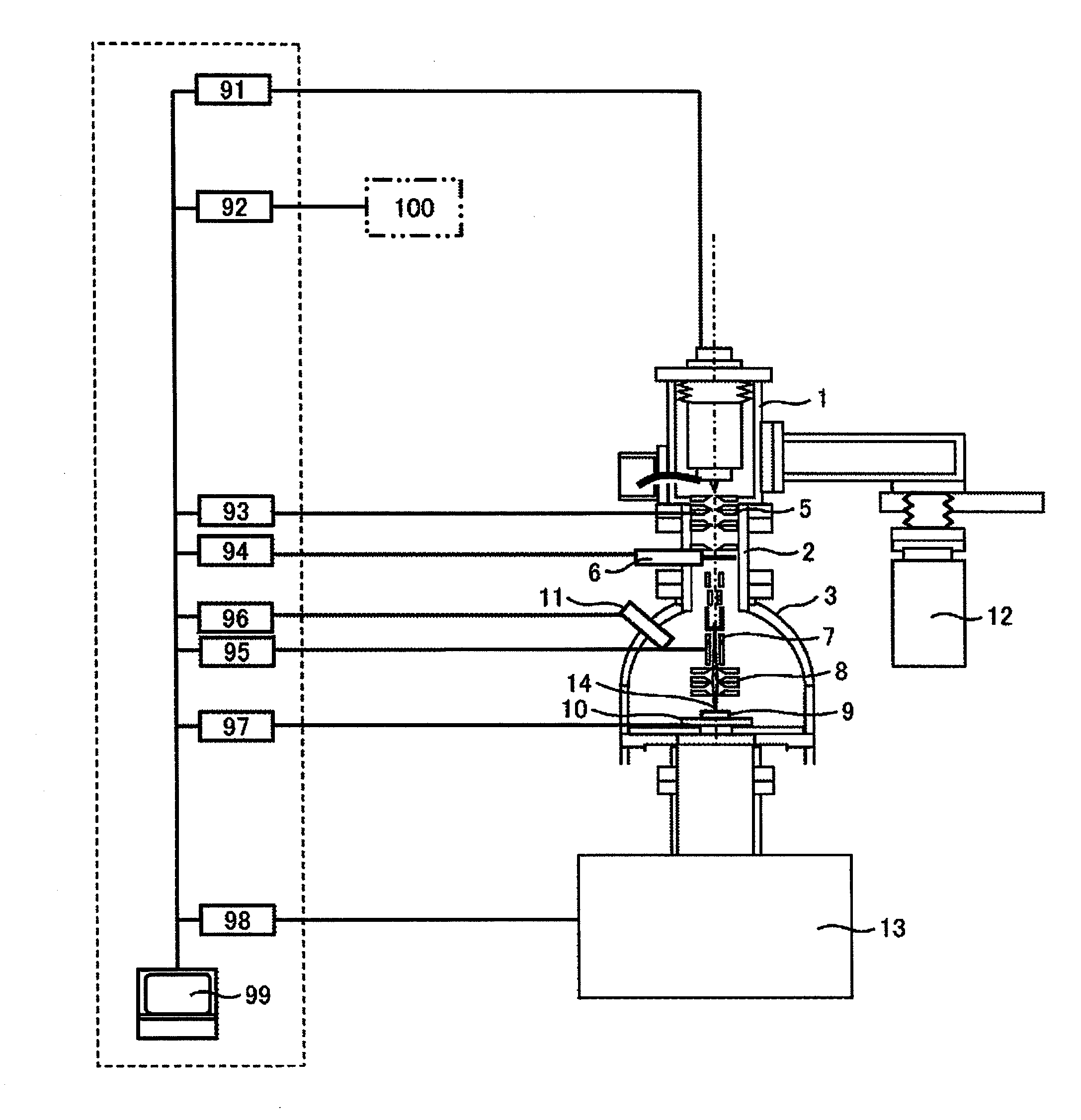
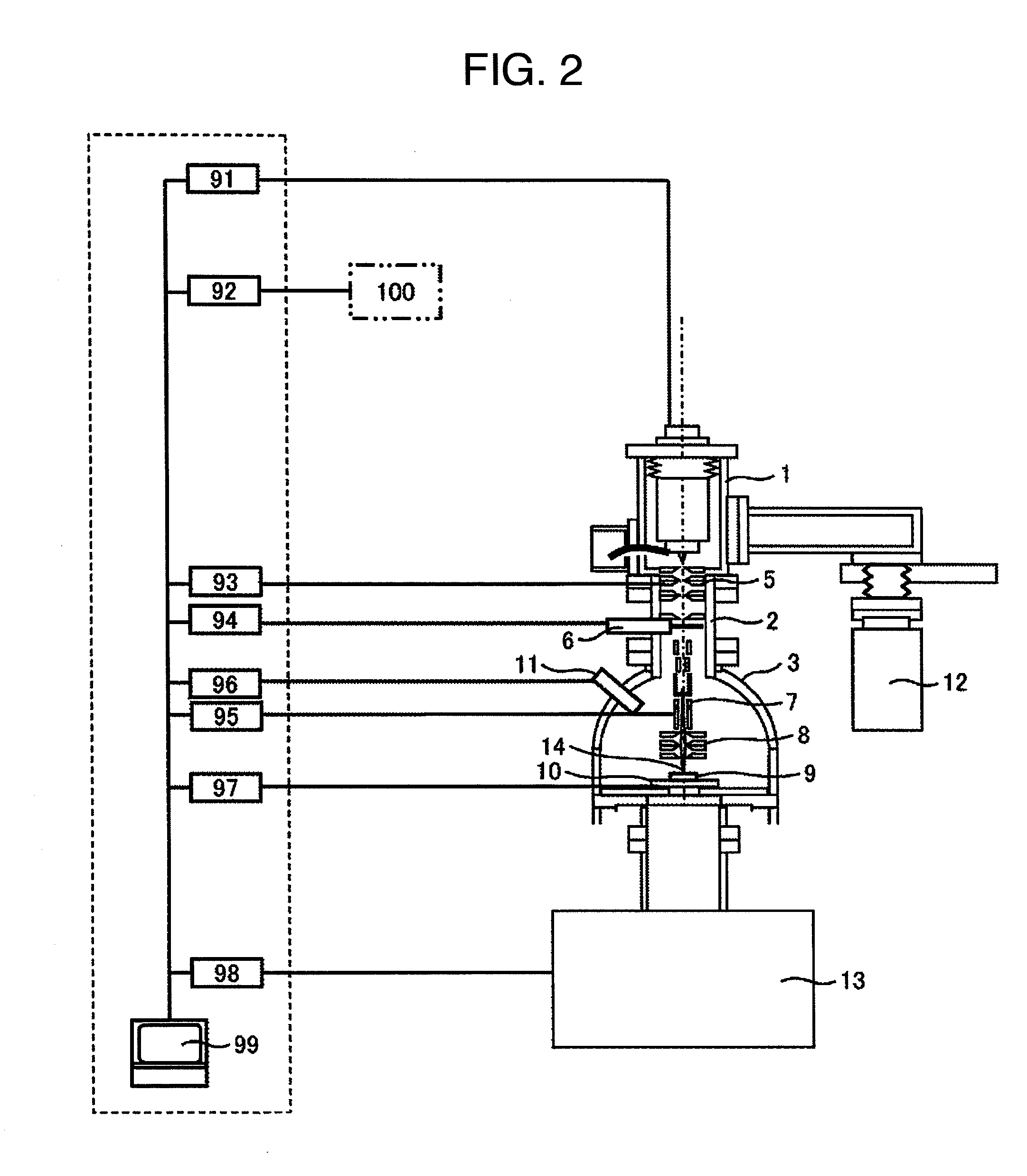
[0072]FIG. 1 shows a schematic structure view of the ion microscope according to this embodiment. This apparatus is comprised of a gas field ionization ion source 1, an ion beam irradiation system column 2, a vacuum sample chamber 3 and the like. The gas field ionization ion source 1 is connected with an end portion 420 of a transfer tube 404 which is one of the component elements of a cooling mechanism 100.
[0073]The ion beam irradiation system column 2 houses therein an electrostatic type condenser lens 5, a beam limiting aperture 6, a beam scanning electrode 7, an electrostatic type objective lens 8 and the like. The vacuum sample chamber 3 houses therein a sample stage 10 for placing a sample 9 thereon, a secondary particle detector 11 and the like. The gas field ionization ion source 1 is provided with an ion source vacuum exhaust pump 12, and the vacuum sample chamber 3 is provided with a sample chamber vacuum exhaust pump 13. The ion beam irradiation system column 2 is kept to...
embodiment 2
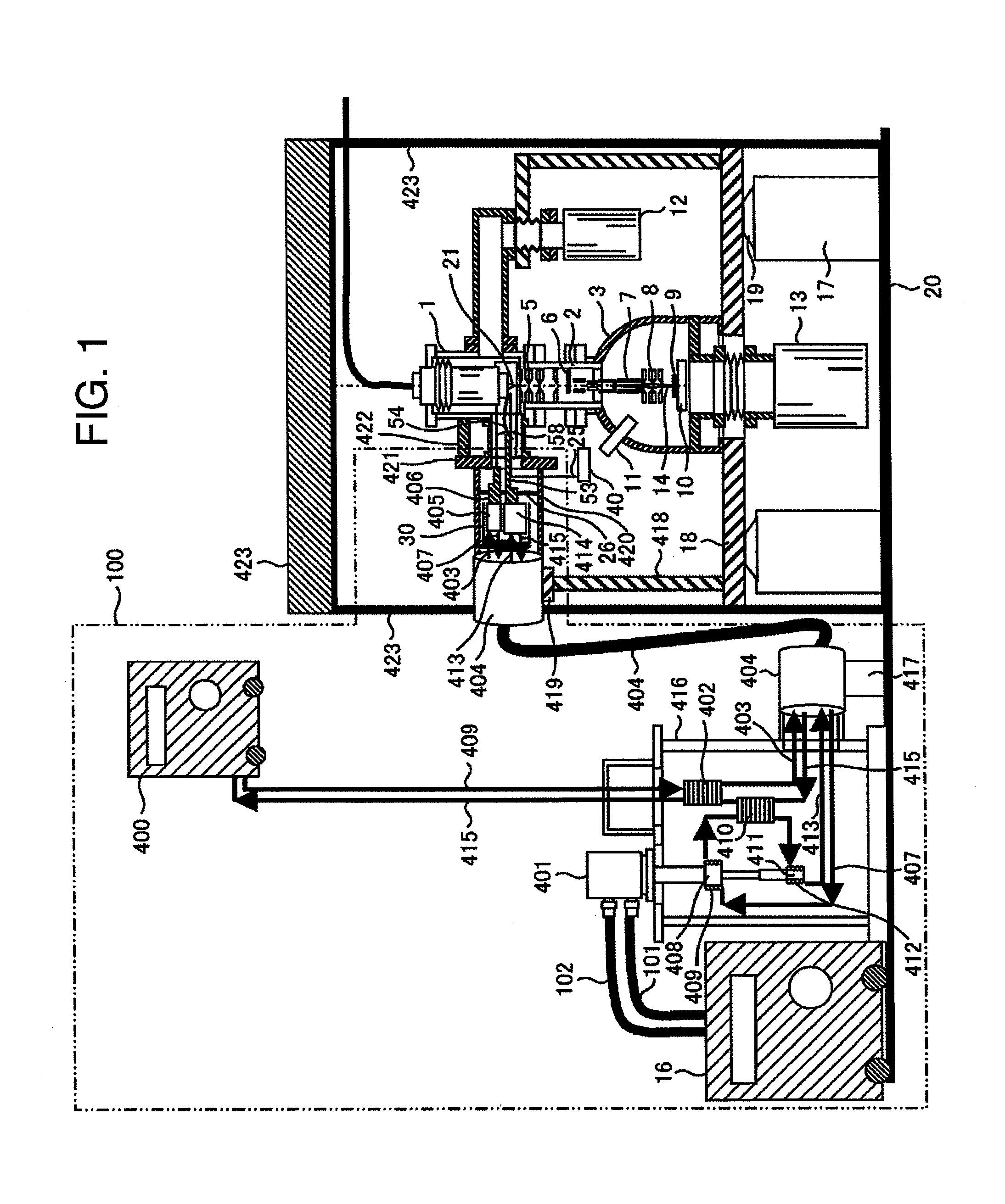
[0115]FIG. 7 shows a schematic structure view of the ion microscope of this embodiment. Differences from Embodiment 1 are mainly described below.
[0116]In this embodiment, to reduce the weight of the transfer tube 404 which is stationarily supported by the gas field ionization ion source 1 and of which load is born by the gas field ionization ion source 1, the transfer tube 404 whose weight is generally large is raised substantially in a vertical direction from vertically below, and a transfer tube portion 430 positioned in widway is stationarily supported by an aperture 27, which is stationarily supported by the apparatus stand 17 directly connected to the floor 20, to support most of the weight of the transfer tube. A transfer tube portion 431 at a leading end portion of the transfer tube portion 430 is stationarily supported by a support 432 stationarily supported by the base plate 18 which has the vibration coming from the floor 20 removed by the vibration removal mechanism 19. V...
embodiment 3
[0118]In this embodiment, a structure that the emitter tip in a normal temperature state can be cooled in a short time is described below. Differences from Embodiments 1 and 2 are mainly described with reference to FIG. 8 and FIG. 9.
[0119]Liquid nitrogen which is a liquefied refrigerant in a liquid nitrogen container 500 is supplied to a pipe 502 via a valve 501. And, it flows through the pipe 403 which is thermally integrated with a radiation shield pipe 503 having a temperature of 80K arranged within the heat-insulated vacuum space of the transfer tube 404, and the pipe 502 which is at least partly connected thermally with a solder 507 or the like. Here, the helium gas as the working gas flowing through the body and inside of the pipe 403 is cooled to thereby cool the radiation shield pipe 503 having a large heat capacity. A leading end of the pipe 502 is U-turned at a leading end of the transfer tube 404, and the nitrogen is flown through a communicated pipe 504, returned into th...
PUM
 Abstract
Description
Claims
Application Information