Electronic imaging apparatus

a technology of electronic imaging and equipment, applied in the field of electronic imaging equipment, can solve the problems of limited downsizing of the entire optical system according, mechanical strength of the system mechanism, and restricted fabrication accuracy, and achieve the effect of wide rang

Inactive Publication Date: 2005-08-23
OLYMPUS CORP
View PDF3 Cites 6 Cited by
  • Summary
  • Abstract
  • Description
  • Claims
  • Application Information

AI Technical Summary

Benefits of technology

[0021]According to the present invention, a slim-design electronic imaging apparatus can be provided which is small

Problems solved by technology

With the progress of the compact design, however, a limit occurs to downsizing of the entire optical system according to compactness of the image sensor.
This is because the physical work of lens elements constituting the optical system, the mechanical strength of a system mechanism, and fabrication accuracy are restricted.
However, this is also restricted because of the maintenance of the b

Method used


Image

  • Electronic imaging apparatus
  • Electronic imaging apparatus
  • Electronic imaging apparatus

Examples


first embodiment

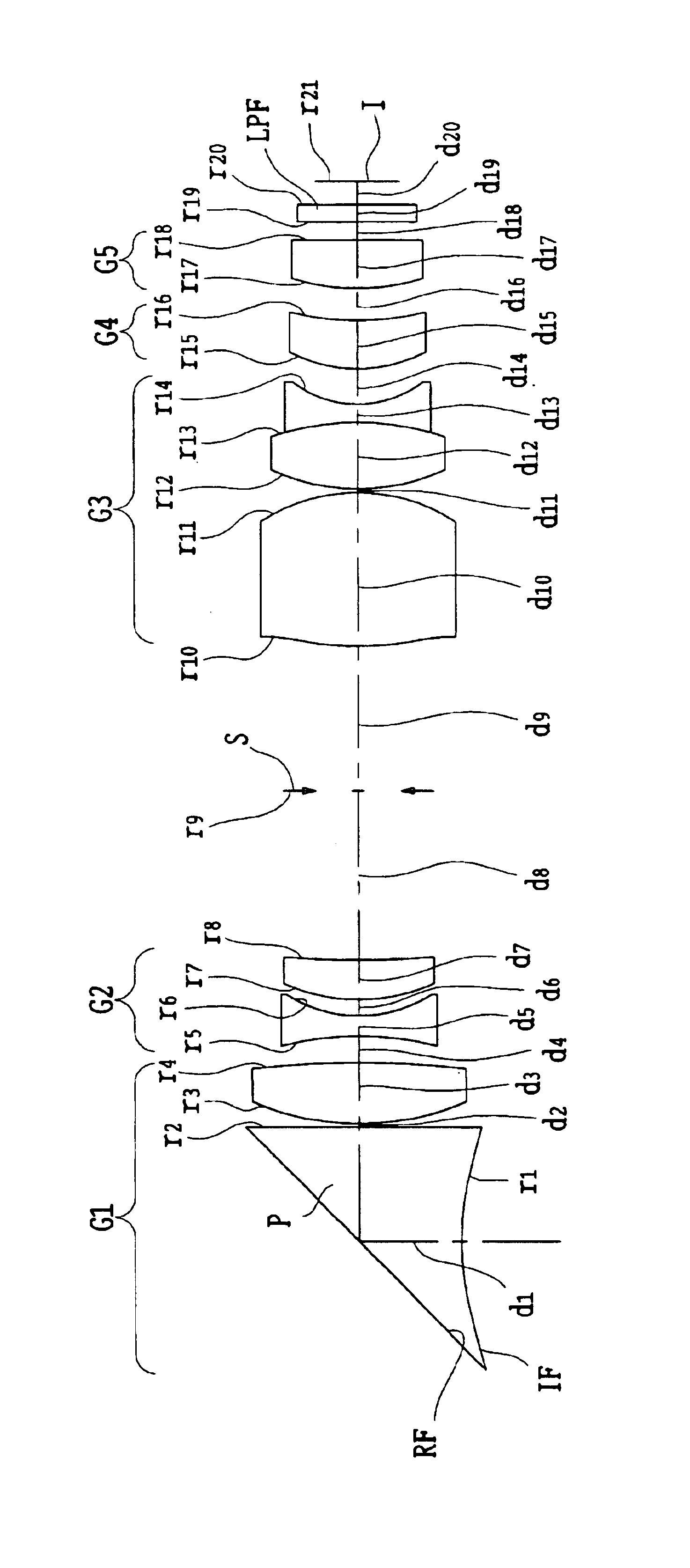
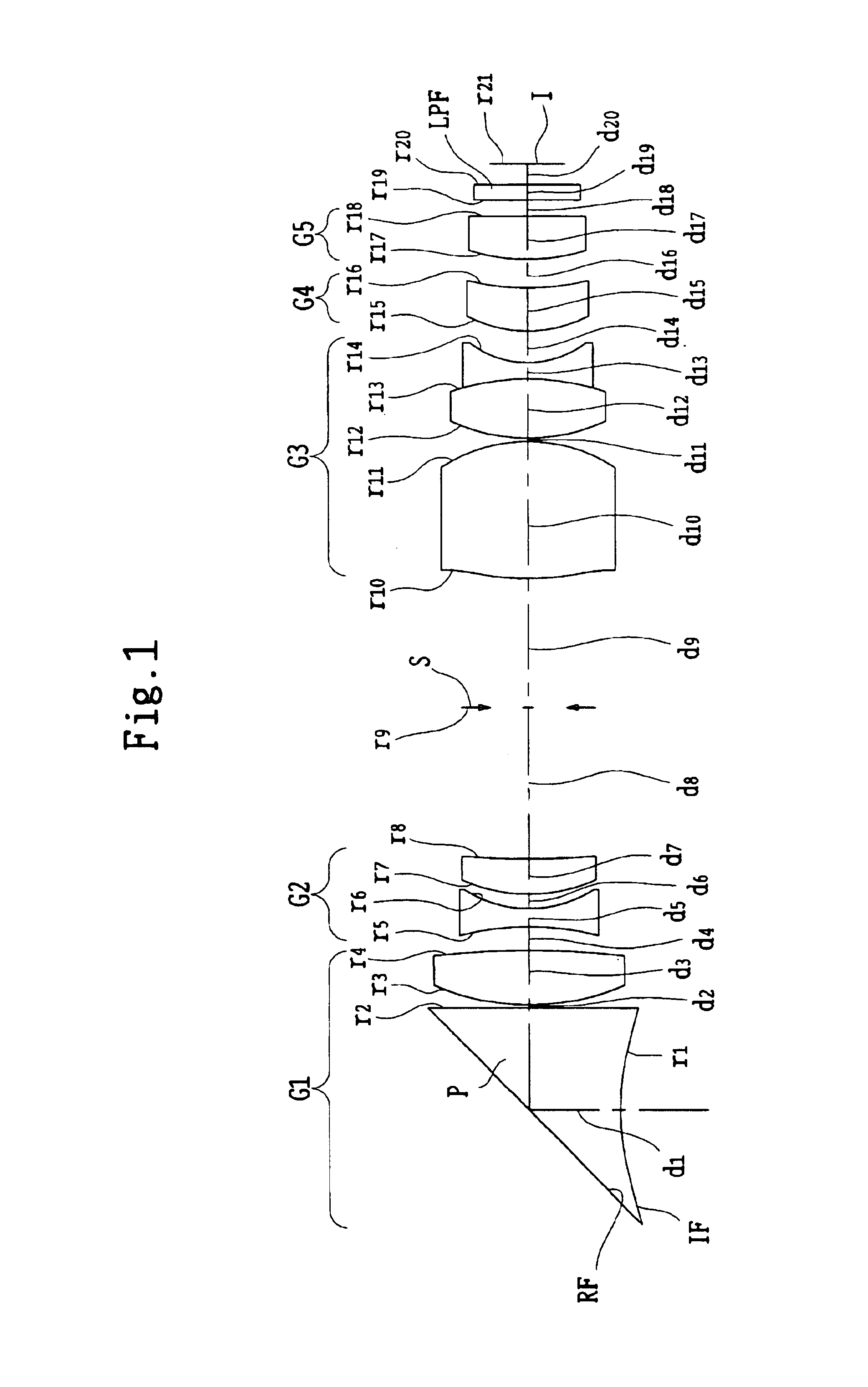
[0055]FIGS. 1 and 2 show optical arrangements in focusing of an infinite object point at the wide-angle position, of the first embodiment of the electronic imaging apparatus. The optical system shown in each figure is a path-bending optical system. In these figures, reference symbol I represents the imaging surface of a CCD which is the electronic image sensor and LPF represents an optical low-pass filter. The electronic imaging apparatus comprises, in order from the object side, the optical system of the present invention, the optical low-pass filter LPF, and the imaging surface I.

[0056]The optical system in the first embodiment comprises, in order from the object side, a first lens unit G1, a second lens unit G2, an aperture stop S, a third lens unit G3, a fourth lens unit G4, and a fifth lens unit G5.

[0057]The first lens unit G1 has the positive refracting power as a whole. The first lens unit G1 includes, in order from the object side, a prism P and a rear lens sub-unit. The pri...

second embodiment

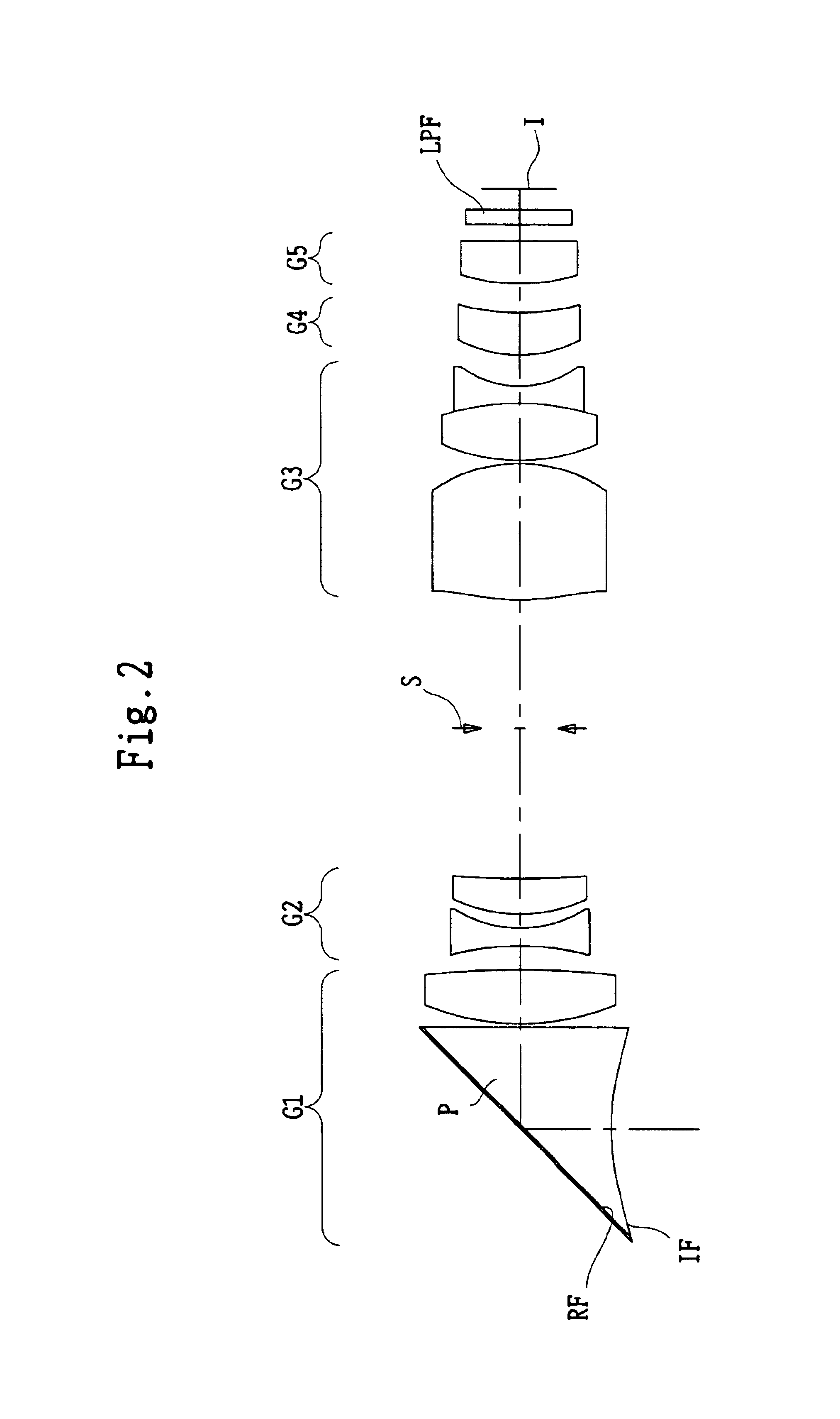
[0067]FIGS. 3 and 4 show optical arrangements in focusing of an infinite object point at the wide-angle position, of the second embodiment of the electronic imaging apparatus. The optical system shown in each figure is a path-bending optical system. The electronic imaging apparatus comprises, in order from the object side, the optical system of the present invention, the optical low-pass filter LPF, and the imaging surface I.

[0068]The optical system in the second embodiment comprises, in order from the object side, the first lens unit G1, the second lens unit G2, the aperture stop S, the third lens unit G3, the fourth lens unit G4, and the fifth lens unit G5.

[0069]The first lens unit G1 has the negative refracting power as a whole. The first lens unit G1 includes, in order from the object side, a positive meniscus lens, the prism P, and a rear lens sub-unit. The prism P has the reflecting surface RF for bending the optical path on the object side. The rear lens sub-unit has the nega...


PUM


Abstract

An electronic imaging apparatus includes an optical system that has a reflecting surface for bending an optical path, and a variable-transmittance optical element placed in the optical system. The variable-transmittance optical element is constructed so that a ray of light passes through the optical element a plurality of times. Whereby, a slim-design electronic imaging apparatus can be provided which is small in size and extremely small in depth and in which the amount of light can be adjusted in a wide range.

Description

BACKGROUND OF THE INVENTION[0001]1. Field of the Invention[0002]This invention relates to an electronic imaging apparatus in which the amount of light is adjusted by a system that the internal transmittance of an optical system is changed.[0003]2. Description of Related Art[0004]Recent electronic imaging apparatuses including digital cameras are progressing in compact or slim design. The compact or slim design largely depends on compactness of an electric circuit or of a recording medium. Consequently, the proportion of an optical system to the entire imaging apparatus is relatively increased. Thus, the optical system, notably a zoom lens, is also progressing in compact design through compactness of an image sensor. For example, a collapsible mount type lens barrel is adopted. The collapsible mount type lens barrel is constructed so that the optical system is shifted outward in photography and is incorporated in the body of the electronic imaging apparatus in carrying.[0005]With the...

Claims


Application Information

Patent Timeline
IPC IPC(8): G02B13/02
CPCG02B13/02
Inventor MIHARA, SHINICHI
Owner OLYMPUS CORP
Why Eureka
Try Eureka