Capacitance measurements for an integrated circuit

a technology of capacitors and integrated circuits, applied in the direction of resistance/reactance/impedence, individual semiconductor device testing, instruments, etc., can solve the problems of increasing the relative importance of wire delay, process flawed, and 4% overall error in time delay modeling

Inactive Publication Date: 2005-08-23
MENTOR GRAPHICS CORP
View PDF7 Cites 38 Cited by
  • Summary
  • Abstract
  • Description
  • Claims
  • Application Information

AI Technical Summary

Problems solved by technology

A relatively large (e.g., 25%) uncertainty in extracting resistance and / or capacitance values results in approximately a 4% overall error in time delay modeling.
However, as device sizes decrease the relative importance of wire delay increases.
The process is flawed because of charge redistribution.
There is, in addition, the uncertainty related to the lack of equality in the capacitance of the transistors on the two sides of the mirror structure.
This additional source of error becomes more significant as the device size decreases.

Method used


Image

  • Capacitance measurements for an integrated circuit
  • Capacitance measurements for an integrated circuit
  • Capacitance measurements for an integrated circuit

Examples


Embodiment Construction

[0021]In the following description, for purposes of explanation, numerous specific details are set forth in order to provide a thorough understanding of the invention. It will be apparent, however, to one skilled in the art that the invention can be practiced without these specific details. In other instances, structures and devices are shown in block diagram form in order to avoid obscuring the invention.

[0022]Reference in the specification to “one embodiment” or “an embodiment” means that a particular feature, structure, or characteristic described in connection with the embodiment is included in at least one embodiment of the invention. The appearances of the phrase “in one embodiment” in various places in the specification are not necessarily all referring to the same embodiment.

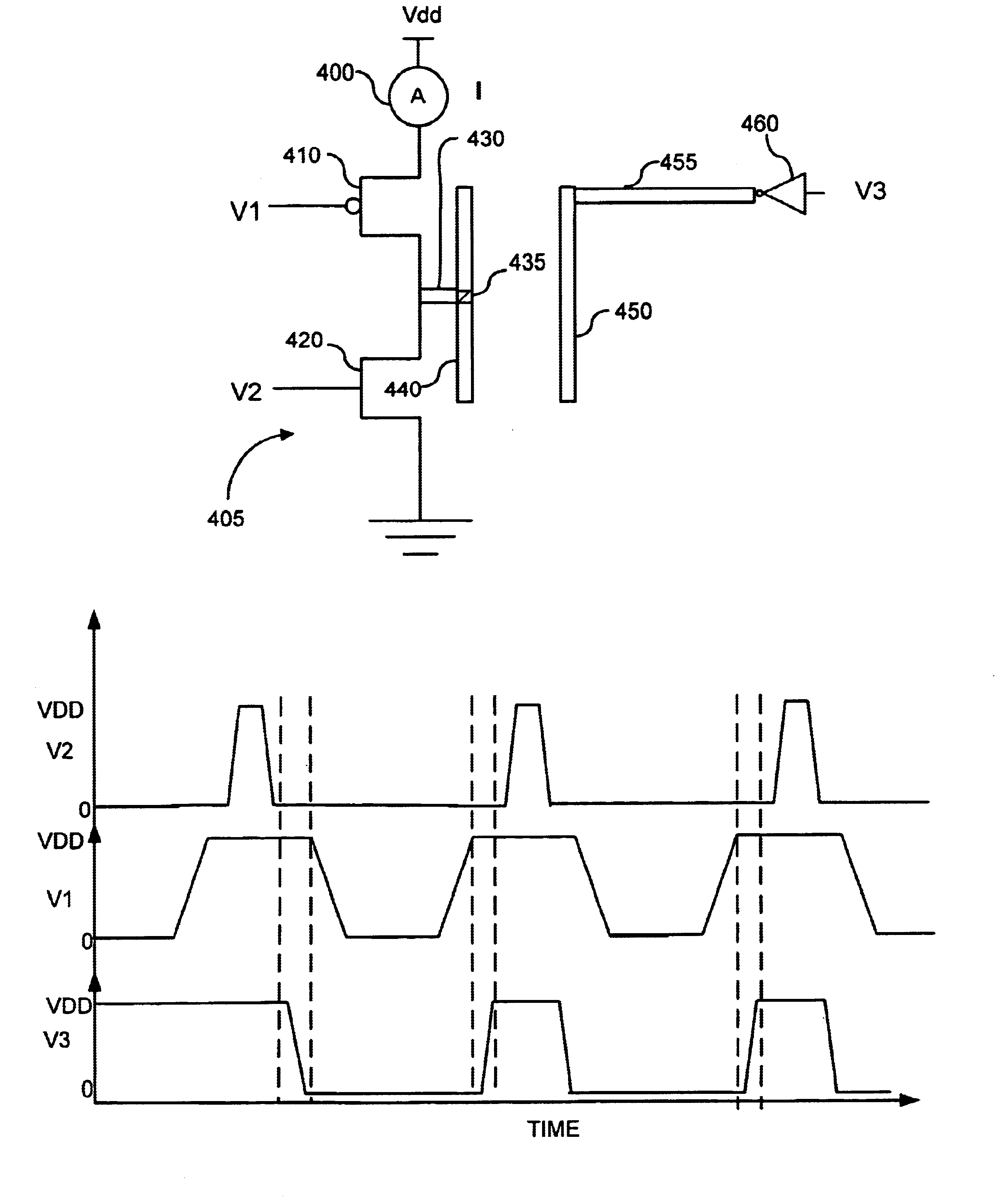
[0023]The invention provides a method and apparatus for determining cross coupling capacitance of wires in an integrated circuit. Total capacitance can be determined by adding the different cross couplin...


PUM


Abstract

A method and apparatus for determining capacitance of wires in an integrated circuit is described. The capacitance information derived according to the invention can be used, for example, to calibrate a parasitic extraction engine or to calibrate an integrated circuit fabrication process. The capacitance information can also be used for timing and noise circuit simulations, particularly for deep sub-Micron circuit design simulations. Briefly, the invention allows measurement of both total capacitance of a line and cross coupling capacitance between two lines by applying predetermined voltage signals to specific circuit elements. The resulting current allows simple computation of total capacitance and cross coupling capacitance. Multiple cross coupling capacitance can be measured with a single device, thus improving the art of library generation, and the overall method is free of uncertainties related to transistor capacitance couplings. The capacitance values obtained can then be used to calibrate procedures, processes, devices, etc.

Description

FIELD OF THE INVENTION[0001]The invention relates to circuit design parameter measurement. More particularly, the invention relates to a method and apparatus for high precision measurement of cross coupling and total capacitance of wires on an integrated circuit design.BACKGROUND OF THE INVENTION[0002]Until the advent of deep sub micron integrated circuit processes, timing behavior of integrated circuits has been dictated by transistor considerations, mostly transistor travel time and the number of logic levels a signal traverses during a clock cycle. Accurate models of transistor device parameters were the key element for the prediction of circuit timing behavior.[0003]For feature sizes larger than 0.35 μm wire delay is typically less than 20% of total timing delay. To account for the 20% contribution to total timing delay high precision delay estimates were not required for wire delay. A relatively large (e.g., 25%) uncertainty in extracting resistance and / or capacitance values re...

Claims


Application Information

Patent Timeline
Patent Type & Authority Patents(United States)
IPC IPC(8): G01R27/26G01R31/28
CPCG01R27/2605G01R31/2822
Inventor SUAYA, ROBERTOGABILLET, SOPHIE H. M.
Owner MENTOR GRAPHICS CORP
Why Eureka
Try Eureka