Optoelectronic package and fabrication method

a technology of optoelectronic packaging and fabrication method, applied in the direction of instruments, optical elements, optical waveguide light guides, etc., can solve the problems of high labor costs and difficult tight spaces

Active Publication Date: 2005-08-30
GENERAL ELECTRIC CO
View PDF15 Cites 14 Cited by
  • Summary
  • Abstract
  • Description
  • Claims
  • Application Information

AI Technical Summary

Problems solved by technology

Each of the different components has different packaging requirements, and efficiently incorporating these different components together in a single module has been a challenge.
Conventional methods have included active part alignment with little or no automation which results in high labor costs.
Modules are often assembled with a hierarchy of solder materials at different temperatures and wire bonding in very difficult tight spaces.

Method used


Image

  • Optoelectronic package and fabrication method
  • Optoelectronic package and fabrication method
  • Optoelectronic package and fabrication method

Examples


Embodiment Construction

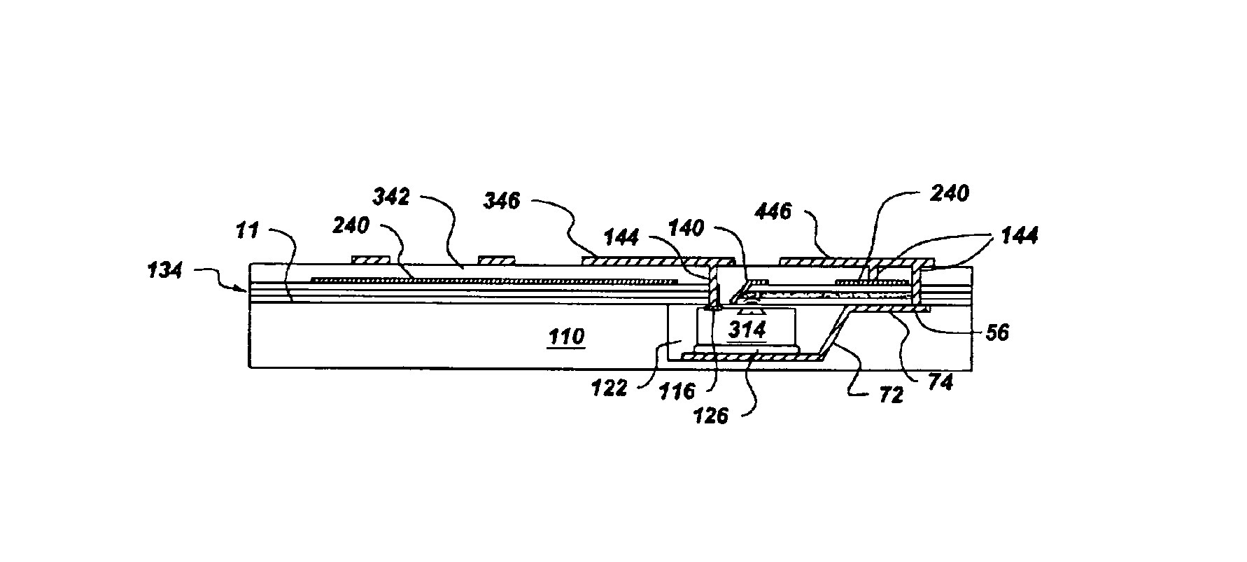
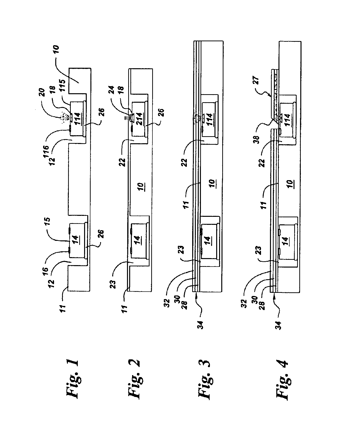
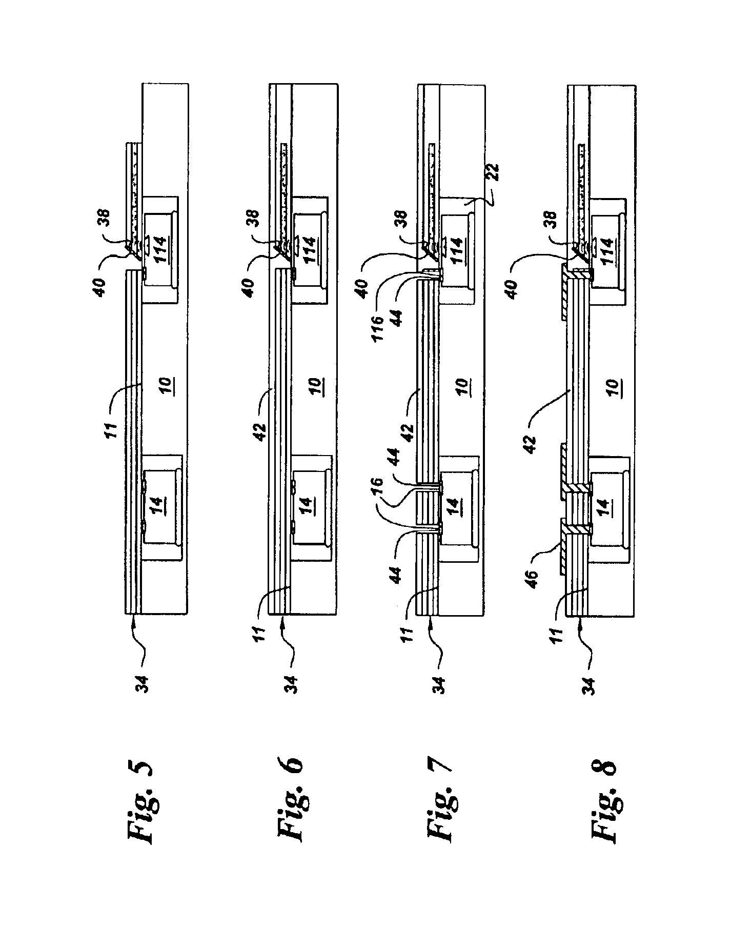
[0012]In accordance with one embodiment of the present invention, a method of fabricating an optoelectronic package 1 (FIG. 10), 101 (FIG. 17), 201 (FIG. 23), 301 (FIG. 20) comprises: (a) positioning an optical device 114, 214, 314, 414, 514 (meaning at least one optical device) within a window 12, 112, 212, 312 of a substrate 10 active-side 115 up and below a top substrate surface 11 (FIGS. 1, 12, 18, and 21); (b) filling the window with an optical polymer material 22, 122, 222, 322 (FIGS. 2, 12, 18, and 22); (c) planarizing surfaces of the optical polymer material and the substrate; (d) patterning waveguide material 34, 134, 234, 334 over the optical polymer material and the substrate to form an optical interconnection path 27 (at least one) and to form a mirror 38 (at least one) to reflect light from the optical device to the interconnection path (FIGS. 3-4, 13-14, 18, 22); and (e) forming a via 44 (at least one) to expose a bond pad 116 of the optical device (FIGS. 7, 15, 18, 22...


PUM


Abstract

An optoelectronic package is fabricated by a method which includes: positioning an optical device within a window of a substrate active-side up and below a top substrate surface; filling the window with an optical polymer material; planarizing surfaces of the optical polymer material and the substrate; patterning waveguide material over the optical polymer material and the substrate to form an optical interconnection path; and to form a mirror to reflect light from the optical device to the interconnection path; and forming a via to expose a bond pad of the optical device.

Description

CROSS REFERENCE TO RELATED APPLICATIONS[0001]This application is related to commonly assigned U.S. patent application Ser. No. 10 / 064,581, filed 29 Jul. 2002, entitled “Method and Apparatus for Fabricating Waveguides and Waveguides Fabricated Therefrom,” which is herein incorporated by reference.BACKGROUND OF INVENTION[0002]Traditional optoelectronic modules include a large number of discrete components such as laser, diodes, fibers, lenses, couplers, electronic driver chips, and signal amplifiers, for example. Each of the different components has different packaging requirements, and efficiently incorporating these different components together in a single module has been a challenge. In single mode waveguide embodiments, for example, optical component attachment typically involves accurate submicron placement (alignment on the order of about 0.25 micrometers) and quick cure adhesives. Conventional methods have included active part alignment with little or no automation which resul...

Claims


Application Information

Patent Timeline
Patent Type & Authority Patents(United States)
IPC IPC(8): G02B6/13G02B6/12G02B6/122G02B6/138G02B6/42
CPCG02B6/12002G02B6/12004G02B6/122G02B6/1221G02B6/138G02B6/42H01L2224/04105H01L2224/32225H01L2224/32245H01L2224/73267H01L2924/15153H01L2924/15192
Inventor SAIA, RICHARD JOSEPHGORCZYCA, THOMAS BERTKAPUSTA, CHRISTOPHER JAMESBALCH, ERNEST WAYNECLAYDON, GLENN SCOTTDASGUPTA, SAMHITADELGADO, ELADIO CLEMENTE
Owner GENERAL ELECTRIC CO
Why Eureka
Try Eureka