
Photonic crystal-based optical waveguide modulator

a technology of optical waveguide and crystal structure, applied in the field of waveguide, can solve the problems of substantial increase in absorption or loss of light energy, and achieve the effect of minimal coupling loss to an output detector

Inactive Publication Date: 2007-01-25
UNITED STATES OF AMERICA AS REPRESENTED BYTHE SEC OF THE ARMY
View PDF4 Cites 8 Cited by
  • Summary
  • Abstract
  • Description
  • Claims
  • Application Information

AI Technical Summary

Benefits of technology

[0011] Accordingly, one object of the present invention is to provide a waveguide that improves spatial economy while significantly diminishing optical loss in the waveguide.
[0013] A further object is to provide a waveguide modulator device that allows for the easy detection of phase modulated light.
[0016] The present invention operates on the basis of linear electromagnetic interference. Its optical guidance is solely due to the presence of photonic band gaps. The core's nonlinear polymer has the sole function of changing the phase of the electromagnetic field—the core does not affect the mode or quality of the waveforms. In addition, the modulator remains single-mode so that coupling losses to an output detector are minimal.

Problems solved by technology

However, in prior art devices, as the distance between the metal plates decreases, absorption or loss of the light energy substantially increases.

Method used


Image

  • Photonic crystal-based optical waveguide modulator
  • Photonic crystal-based optical waveguide modulator
  • Photonic crystal-based optical waveguide modulator

Examples


Embodiment Construction

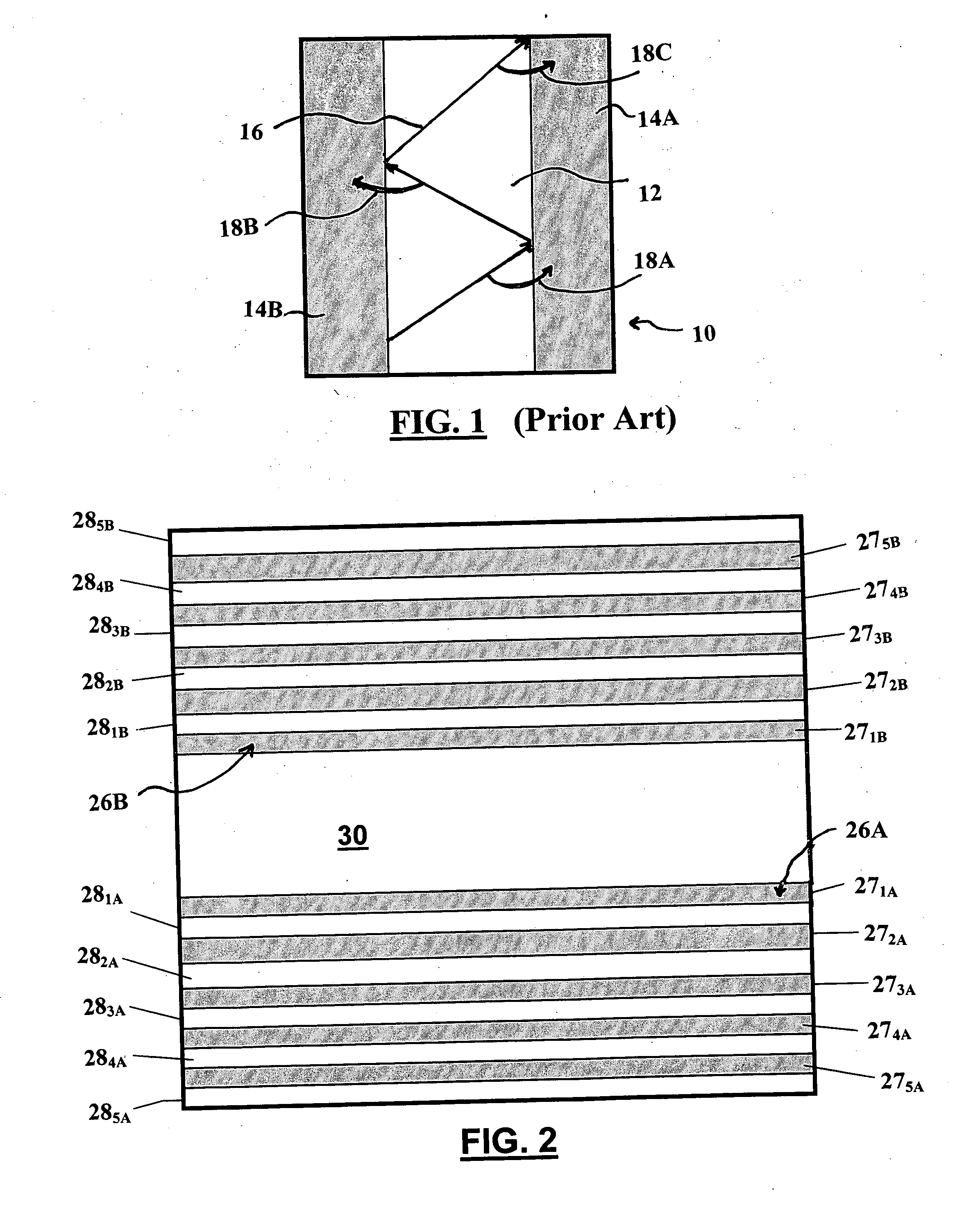
[0028] Referring now to the drawings, wherein like reference numerals designate identical or corresponding parts throughout the several views, and, more particularly to FIG. 2, a core 30 formed from a non-linear optical polymer (NLOP) is centrally positioned between a lower cladding region 26A and an upper cladding region 26B. The core has a linear refractive index of n0.

[0029] The upper cladding region has a plurality of layers 271B, 281B, 272B, 282B, 273B, 283B, 274B, 284B, 275B, and 285B that are positioned one on top of the other. Correspondingly, the bottom cladding region has stacked layers 271A, 281A, 272A, 282A, 273A, 283A, 274A, 284A, 275A, and 285A. Layers 271B, 271A, 272B, 272A, 273B, 273A, 274B, 274A, 275B, and 275A have a linear refractive index of n1 and layers 281B, 281A, 282B, 282A, 283B, 283A, 284B, 284A, 28%B, and 285A have a linear refractive index of n2.

[0030] Thus, the stacked cladding layers are positioned such that the first layers next to the core 30 have a...


PUM


Abstract

A waveguide has upper and lower cladding regions. A core of the waveguide made of a non-linear optical polymer is positioned between the upper and lower cladding regions. A first electrode is connected to the upper cladding region and a second electrode is connected to the lower cladding region. The upper cladding region and the lower cladding region are made of photonic band gap materials and have multiple periods of cladding layers with each period having a first layer having a linear refractive index of n1 and each period having a second layer having a linear refractive index of n2. The waveguide allows for minimal distances to exist between the electrodes while allowing for virtual lossless cm-long transmission of propagating light. By applying a voltage to the electrodes, the propagated light can be modulated.

Description

DEDICATORY CLAUSE [0001] The invention described herein may be manufactured, used and licensed by or for the U.S. Government for governmental purposes without payment of any royalties thereon. BACKGROUND OF THE INVENTION [0002] 1. Field of the Invention [0003] This invention pertains to the field of photonic bandgap technology. More particularly, the invention pertains to a waveguide that permits the virtually lossless unidirectional propagation and phase shift of light. [0004] 2. Discussion of the Background [0005] Over the past couple of decades, active and passive devices ranging from optical switches to complex integrated networks have been developed in the data communication and optics industries [0006] Recently, the data communications and optics industries have experienced high demand for various types of small-scale opto-electronic devices. The importance of optical waveguides for both single and multi-mode transmission is unquestionable—particularly in the 1.3-1.6 μm region...

Claims


Application Information

Patent Timeline
Patent Type & Authority Applications(United States)
IPC IPC(8): G02B6/10
CPCB82Y20/00G02F2202/32G02F1/065G02B6/1225
Inventor BLOEMER, MARK J.SCALORA, MICHAELPOLIAKOV, EVGENI Y.
Owner UNITED STATES OF AMERICA AS REPRESENTED BYTHE SEC OF THE ARMY
Learn More