Integrated semiconductor optical device

a semiconductor optical and integrated technology, applied in the direction of optical elements, semiconductor lasers, instruments, etc., can solve the problems of increasing the length of the device, complicating the processing process, and causing so as to suppress the coupling loss of guided light and suppress the output of emitted light

Inactive Publication Date: 2011-04-21
SUMITOMO ELECTRIC IND LTD
View PDF2 Cites 8 Cited by
  • Summary
  • Abstract
  • Description
  • Claims
  • Application Information

AI Technical Summary

Benefits of technology

[0010]In the integrated semiconductor optical device according to the present invention, in the first semiconductor optical device, light propagates through the first optical waveguide including the first lower cladding layer, the first core layer, and the first upper cladding layer. In the second semiconductor optical device, light propagates through the second optical waveguide including the second lower cladding layer, the second core layer, and the second upper cladding layer. The first adjusting layer has a refractive index between the refractive index of the first core layer and the refractive index of the first buried layer. The first adjusting layer extends in the direction of the predetermined axis. The first adjusting layer is in contact with the first ridge portion. The first adjusting layer may be formed so as to have a width that is constant from the first end facet to the joint boundary. By adding the first adjusting layer so as to be next to the first ridge portion in the first semiconductor optical device, the optical confinement of guided light in a direction (hereafter, also referred to as a first direction) orthogonal to the direction in which the first lower cladding layer, the first core layer, and the first upper cladding layer are stacked and the direction of the predetermined axis is reduced. As a result, the beam profile of guided light in the first semiconductor optical device is broadened in the first direction. In contrast, the beam profile of guided light in the first semiconductor optical device in a direction (hereafter, also referred to as a second direction) orthogonal to the direction of the predetermined axis and parallel to the direction in which the first lower cladding layer, the first core layer, and the first upper cladding layer are stacked is conversely narrowed due to the broadened profile in the first direction. Thus, the beam profile in the first semiconductor optical device is made close to the beam profile in the second semiconductor optical device. As a result, the difference between the beam profile of guided light in the first semiconductor optical device and the beam profile of guided light in the second semiconductor optical device can be reduced. Adjustment can be performed such that the effective refractive index of the first optical waveguide and the effective refractive index of the second optical waveguide are substantially equal to each other. Accordingly, scattering or reflection of guided light at the butt-joint joint interface between the first semiconductor optical device and the second semiconductor optical device can be reduced. Thus, coupling loss of guided light can be suppressed without a tapering region.
[0021]In this integrated semiconductor optical device, since the first adjusting layer is provided, scattering or reflection of guided light at the butt-joint joint interface between the first semiconductor optical device and the second semiconductor optical device can be reduced. Thus, coupling loss of guided light can be suppressed without a tapering region. Therefore, degradation of device characteristics such as degradation of the beam profile of guided light and a decrease in the output of emitted light can be suppressed.

Problems solved by technology

Accordingly, when a plurality of semiconductor optical devices having optical waveguides that have different structures or are composed of different materials are joined together by a butt joint method, coupling loss of guided light is caused by reflection at the joint boundary of the semiconductor optical devices.
However, the addition of the tapering region results in an increase in the device length.
Furthermore, the addition of the tapering region requires an extra process, which complicates the processing process.
Accordingly, in the integrated semiconductor optical device described in Patent Document 1, it is difficult to achieve a decrease in the size of the device and a decrease in the cost.

Method used


Image

  • Integrated semiconductor optical device
  • Integrated semiconductor optical device
  • Integrated semiconductor optical device

Examples


first embodiment

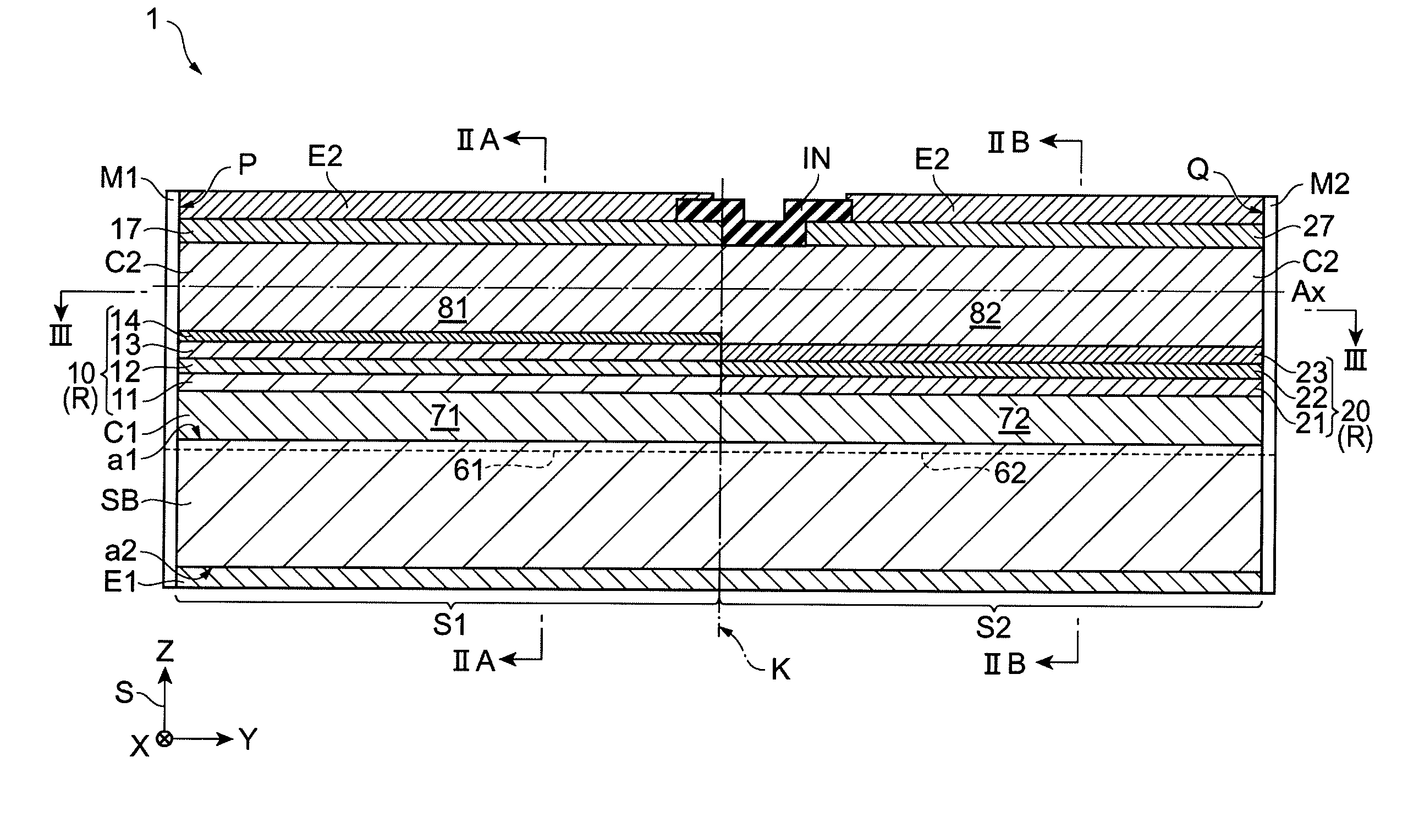
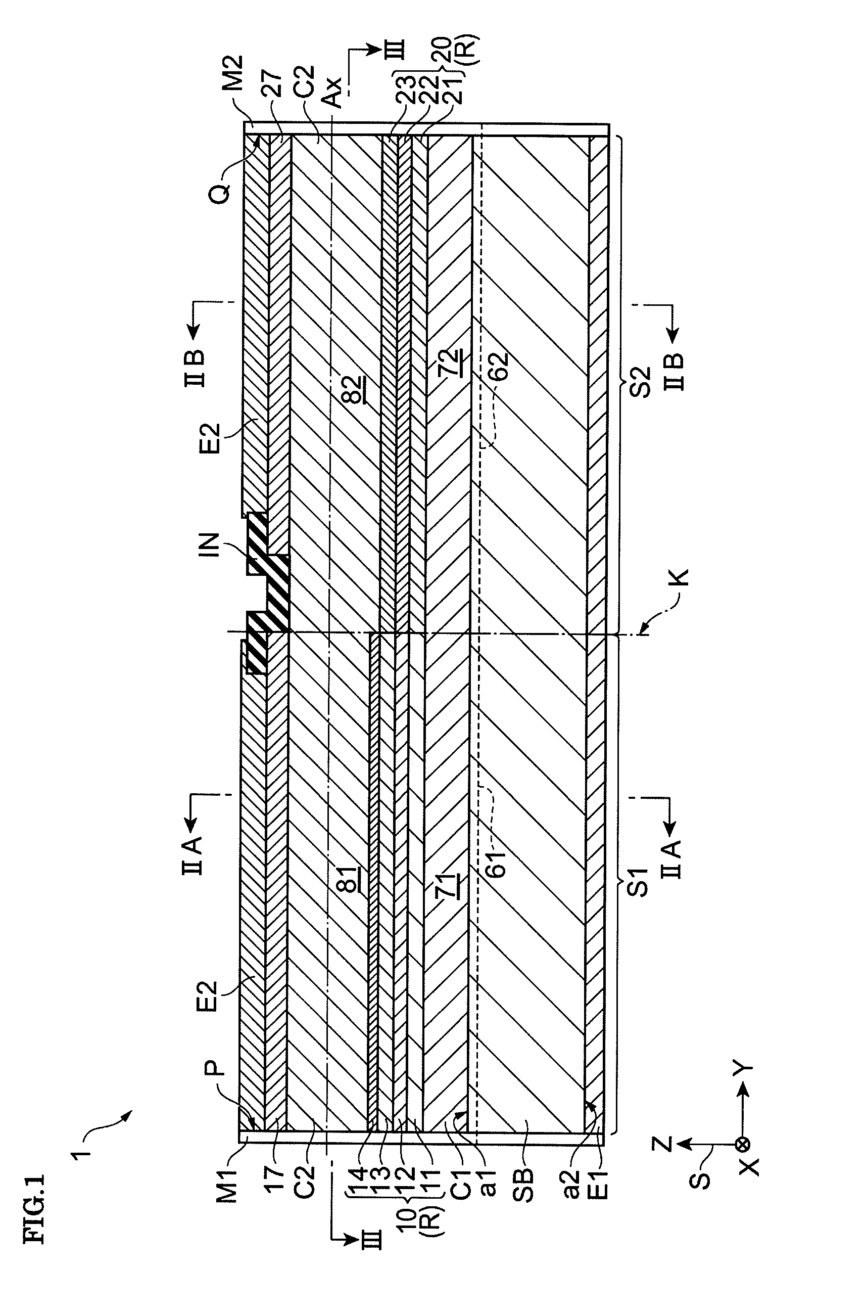
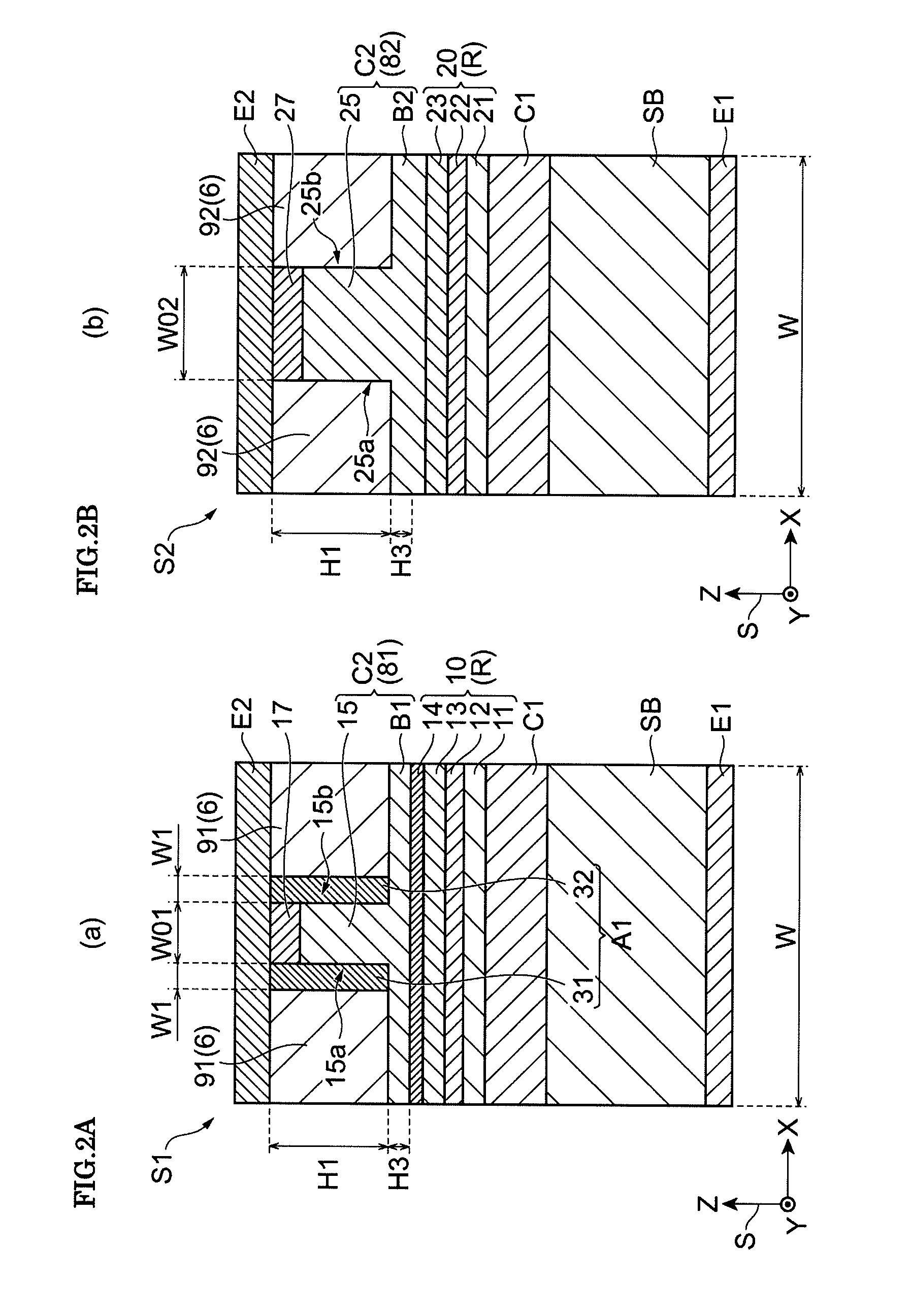
[0042]FIG. 1 is a sectional view schematically illustrating an integrated semiconductor optical device 1. FIG. 2A is a sectional view taken along line IIA-IIA in FIG. 1. FIG. 2B is a sectional view taken along line IIB-IIB in FIG. 1. FIG. 3 is a sectional view taken along line in FIG. 1.

[0043]Referring to FIG. 1, the integrated semiconductor optical device 1 includes a first semiconductor optical device S1 and a second semiconductor optical device S2. The first semiconductor optical device S1 is, for example, a semiconductor light emitting device such as a distributed feedback (DFB) laser diode. The second semiconductor optical device S2 is, for example, an electro-absorption (EA) optical modulator. The first semiconductor optical device S1 and the second semiconductor optical device S2 are optically joined together at a joint boundary K by a butt joint method.

[0044]In the integrated semiconductor optical device 1, the first semiconductor optical device S1 and the second semiconduct...

second embodiment

[0103]Hereinafter, an integrated semiconductor optical device according to a second embodiment will be described with reference to FIGS. 14A, 14B, 15, and 16A to 16D. FIGS. 14A and 14B are sectional views illustrating a modification of the configurations in FIGS. 2A and 2B. FIG. 15 is a sectional view illustrating a modification of the configuration in FIG. 3. FIGS. 16A to 16D illustrate examples of a beam intensity distribution of guided light. The only difference of the integrated semiconductor optical device according to the second embodiment from the integrated semiconductor optical device 1 according to the first embodiment is an adjusting layer. Thus, descriptions other than the adjusting layer are omitted.

[0104]Referring to FIG. 14A, like the first semiconductor optical device S1 according to the first embodiment, the first semiconductor optical device S1 according to the second embodiment includes the first adjusting layer A1. Referring to FIG. 14B, unlike the second semicon...

third embodiment

[0120]Hereinafter, an integrated semiconductor optical device according to a third embodiment will be described with reference to FIGS. 17A, 17B, and 18. FIGS. 17A and 17B are sectional views illustrating a modification of the configurations in FIGS. 2A and 2B. FIG. 18 is a sectional view illustrating a modification of the configuration in FIG. 3. The only differences of the integrated semiconductor optical device according to the third embodiment from the integrated semiconductor optical device according to the first embodiment are adjusting layers. Thus, descriptions other than the adjusting layers are omitted.

[0121]Referring to FIG. 17A, a first semiconductor optical device S13 of the integrated semiconductor optical device according to the third embodiment includes a third adjusting layer A3 in addition to the first adjusting layer A1. The third adjusting layer A3 includes a fifth portion 35 and a sixth portion 36 that extend in the direction of the predetermined axis Ax. The fi...


PUM

PropertyMeasurementUnit
widths W1aaaaaaaaaa
lengthaaaaaaaaaa
lengthaaaaaaaaaa

Abstract

An integrated semiconductor optical device includes first and second semiconductor optical devices. The first semiconductor optical device includes a first core layer, a first upper cladding layer including a first ridge portion, a first buried layer surrounding the first ridge portion, and a first adjusting layer provided between the first buried layer and the first ridge portion. The second semiconductor optical device includes a second core layer, a second upper cladding layer including a second ridge portion. The first semiconductor optical device and the second semiconductor optical device are arranged next to each other in a predetermined axis direction. The first core layer is joined to the second core layer by a butt joint method at a joint boundary between the first and second semiconductor optical devices. The first adjusting layer has a refractive index lower than a refractive index of the first core layer and higher than a refractive index of the first buried layer. The first adjusting layer extends in the predetermined axis direction. The first adjusting layer has a constant width from one end facet to the joint boundary.

Description

BACKGROUND OF THE INVENTION[0001]1. Field of the Invention[0002]The present invention relates to an integrated semiconductor optical device used for optical communication, optical recording, optical measurement, or the like.[0003]2. Description of the Related Art[0004]In recent years, an integrated semiconductor optical device in which a gain region (light emitting region) or a semiconductor laser device and another semiconductor optical device such as an optical modulator, an optical amplifier, or an optical multiplexer and demultiplexer are integrated on a single semiconductor substrate has been developed. To couple a semiconductor laser device with another semiconductor optical device optically, for example, a butt joint method is employed. Japanese Unexamined Patent Application Publication No. 2008-66318 (Patent Document 1) describes a semiconductor wavelength tunable laser in which a gain region and a ring resonator have been joined together by a butt joint method. In this semi...

Claims


Application Information

Patent Timeline
Patent Type & Authority Applications(United States)
IPC IPC(8): G02F1/025G02B6/122H01S5/12
CPCB82Y20/00G02B6/42G02B6/4203G02B2006/12097G02F1/01708H01S5/34306H01S5/1014H01S5/12H01S5/222H01S5/2224H01S5/2231H01S5/0265
Inventor HASHIMOTO, JUN-ICHI
Owner SUMITOMO ELECTRIC IND LTD
Why Eureka
Try Eureka