Manufacturing method for an electrophoretic display

a manufacturing method and electrophoretic technology, applied in the direction of liquid/fluent solid measurement, fluid pressure measurement, peptide, etc., can solve the problems of low energy and long time required manufacturing process, inferior liquid crystal material, and small window for manufacturing process

Inactive Publication Date: 2005-03-03
IND TECH RES INST
View PDF3 Cites 8 Cited by
  • Summary
  • Abstract
  • Description
  • Claims
  • Application Information

AI Technical Summary

Problems solved by technology

When performing the second exposure, the low energy and long time manufacturing process is required.
This may make the liquid crystal material inferior.
In addition, the window for the manufacturing process is small and the yield is low, and the applicable display modes are fewer.
Besides, because the conditions for the manufacturing process and the display characteristics of the liquid crystal display are not easily controlled.

Method used


Image

  • Manufacturing method for an electrophoretic display
  • Manufacturing method for an electrophoretic display
  • Manufacturing method for an electrophoretic display

Examples


first embodiment

[0018] First, please refer to FIG. 2A to 2M. FIG. 2A to 2M are the perspective diagrams of a manufacturing process for a single substrate electrophoretic display according to the present invention. The process comprises the following steps.

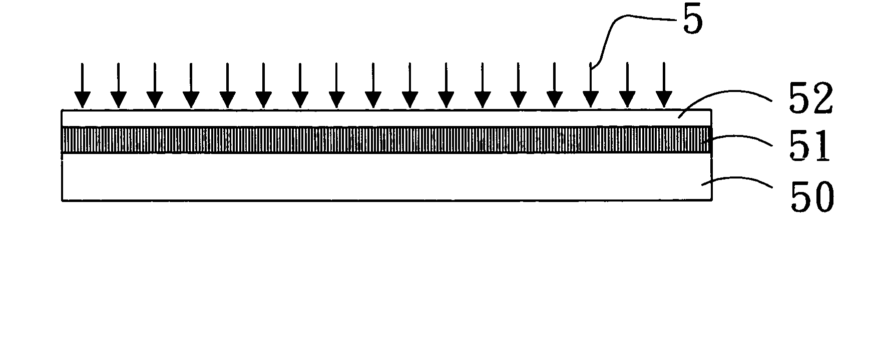
[0019] Please refer to FIG. 2A to 2D. FIG. 2A to 2D are the perspective diagrams of a manufacturing process for a first board. In FIG. 2A, a buffer layer 51 is manufactured on an auxiliary substrate 50. In FIG. 2B, an optical polymer material layer 52 (such as NOA65 / NOA72 optical polymer material) is coated on the buffer layer 51. In FIG. 2C, ultraviolet rays 5 are irradiated for performing the exposure manufacturing process. In FIG. 2D, ultraviolet rays 5 are used for solidifying the optical polymer material 52 so as to form polymer 52′. The above is the manufacturing process for making the first board 530.

[0020]FIG. 2E to 2I are the perspective diagrams of a manufacturing process for a second board. In FIG. 2E, electrode patterns 540 are manufa...

fifth embodiment

[0037] In FIG. 6J, the first board 630 is reversely positioned on the second board 660. After they are aligned with each other, the exposure process is performed. In FIG. 6K, the exposure manufacturing process of the ultraviolet rays 5 is performed. After the exposure manufacturing process of the ultraviolet rays 5, the mixture 68′ composed of the charged pigment articles 63, the intervals 661 and a few amount of optical polymer material is separated so as to combine the first board 630 with the second board 660. In FIG. 6L, the first board 630 is combined with the second board 660, and the charged pigment particles 63 are separated from the optical polymer material. Therefore, the charged pigment particle solution 69 is fully confined by the polymer. In FIG. 6M, the auxiliary substrate 60 and the buffer layer 61 of the first board 630 are stripped, and the auxiliary substrate 70 and the buffer layer 61 of the second board 660 are also stripped. Therefore, the manufacturing of the e...

sixth embodiment

[0042] In the present invention, the display has no intervals and has no substrates. Similarly, due to omission of substrates, the electrophoretic display can be flexibly pasted and positioned on an object. For example, the electrophoretic display without substrate can be pasted on clothing, newspaper, windscreen, wall, book or file wrapper so as to form a freely pasted electrophoretic display.

[0043] In the first to sixth embodiments, the optical polymer material can be photocurable resin. In the electrophoretic display of the present invention, the optical polymer material mixture is composed of optical polymer material and charged pigment particle solution. This is very different from the liquid crystal material. Furthermore, polymer walls formed by the optical polymer material can be closed matrix polymer walls or non-closed matrix polymer walls.

[0044] In addition, in the second to the sixth embodiments, the molding method for forming the polymer walls can be cooperated with hea...


PUM

PropertyMeasurementUnit
electric conductionaaaaaaaaaa
hydrophobicaaaaaaaaaa
thicknessaaaaaaaaaa

Abstract

a manufacturing method for an electrophoretic display applying optical polymer material is provided. The main characteristic is that the charged pigment particles are confined with optical polymer material so as to achieve electrophoretic display. In the manufacturing process, a first layer of optical polymer material is coated on an auxiliary substrate having a buffer layer for performing an optical polymerization manufacturing process. After the polymerization, on the first layer of the optical polymer material layer, the manufacturing process required by the electrophoretic display is further performed. After a second layer of optical polymer material is coated on a substrate required by the electrophoretic display having a plurality of electrode patterns, by using a mask exposure, the optical polymer material is solidified to form a polymer wall, or a molding method is applied with ultraviolet irradiation for solidifying the optical polymer material so as to form the polymer wall. Next, in a hole formed by the polymer wall, the mixture formed by the charged pigment particles and a few amount of optical polymer material is filled, and the auxiliary substrate is aligned with the substrate so as to perform the mask exposure polymerization manufacturing process. Therefore, the auxiliary substrate is combined with the substrate. Finally, the auxiliary substrate is stripped out so as to finish the manufacturing of a single substrate electrophoretic display.

Description

BACKGROUND OF THE INVENTION [0001] 1. Field of the Invention [0002] The present invention relates to a manufacturing method for an electrophoretic display to reduce the thickness and weight of the display, and particularly, to a manufacturing method applied to a flexible plastic substrate. In addition, the method has fewer steps for manufacturing process, and the conditions for the manufacturing process are more easily controlled. Furthermore, the display has various modes. [0003] 2. Description of the Prior Art [0004] As the personal digital electricity products are more and more popular, the portable display panels are developed from the seven segment digit display in the early days to colorful multi-media display panels nowadays. Obviously, it is more and more important to apply the displays in the personal digital communication products. The displays to be applied in the portable digital products must have the following requirement: to be colorful, to be capable of saving electr...

Claims


Application Information

Patent Timeline
Patent Type & Authority Applications(United States)
IPC IPC(8): G02F1/167G02F1/16755G02F1/1679
CPCG02F1/167G02F1/1679G02F1/16755
Inventor LIAO, CHI-CHANGLIU, KANG-HUNGHSIN, LUNG-PINWONG, YI-CHUNSHA, YI-ANCHAN, CHING-HSIANGSHEU, CHIA-RONGWU, CHUNG-WENLIN, YAO-SHENG
Owner IND TECH RES INST
Why Eureka
Try Eureka