Inertia sensor

a sensor and inertia technology, applied in the field of inertia sensors, can solve the problems of inaccuracy in crystal alignment, limitation of etching width, and arrangement of lateral electrodes, and achieve the effect of reducing the number of lateral electrodes

Inactive Publication Date: 2005-09-06
IND TECH RES INST
View PDF2 Cites 2 Cited by
  • Summary
  • Abstract
  • Description
  • Claims
  • Application Information

AI Technical Summary

Benefits of technology

[0023]The secondary objective of the invention is to provide an inertia sensor capable of realizing the designing goal of high aspect ratio structure, and its cost is also cheaper than that of other process of high aspect ratio.
[0026]The further another objective of the invention is to provide an inertia sensor wherein, on one hand, it has reinforcing structure for suspension structure, on the other hand, it may suppress or change the vibration mode.

Problems solved by technology

Currently, the bulk micromachining is mostly applied in the design of inertia sensor, but such kind of designing manner is always incurred with the inaccurate alignment in the crystal direction of single crystal silicon substrate and the limitation in etching width.
In addition, if the lateral sensing or signal driving arrangement is required, the arrangement of lateral electrodes is another troublesome problem.
1. For deep RIE, it is applying two major gases to protect the side wall and to etch at the same time, such that the purpose to etch the materials vertically is reached, but there are some inherent limitations on such kind of manufacturing manner technique: first, the etched materials must be silicon based, such that the purpose for protecting the side wall may be reached; if the size difference of each zone to be etched is large, the etched depths will be very differentiated as well, so it is impossible to reach equal-depth etching; in addition, although the micro intervals can be generated by the etching processes, it is impossible for other techniques to manufacture electrodes on side surfaces.
2. For bulk silicon anisotropic etching, it mostly applies the different etching speeds of etching liquid on the crystal lattice of single crystal silicon to reach the purpose of anisotropic etching, so the etching and non-etching areas defined prior to the etching process become a crucial factor for the accurate alignment on the original crystal lattice of single crystal silicon; furthermore, controlling the etching uniformity of entire wafer is also a big problem.
3. For LIGA process, it combines the lithography, electroforming , and molding to manufacture microstructure with high accuracy and high aspect ratio; the standard LIGA technique applies synchrotron radiation X ray as lithography, and the accuracy of the microstructure may reach sub-micro level, but it is expensive and complicated, so it has developed a trend for applying ultraviolet light, laser, or plasma as light source for LIGA-like technique and, since UV lithography process incorporated with thick film photo-resist technique may realize an UV-LIGA process of low cost.
In the future, MEMS will march into the field of dynamic system, so how to promote the strength for sensing signals and how to control different sensing levels have become a very difficult challenge.

Method used


Image

  • Inertia sensor
  • Inertia sensor
  • Inertia sensor

Examples


Embodiment Construction

[0035]Please refer FIG. 5, which shows an embodiment for an inertia sensor according to the invention. The inertia sensor 30 is comprised of a suspension structure 31 and a micro-electroplating structure 32. The suspension structure 31 has an arm 311, one side 3111 of which is connected to a supporting piece 33, and another side 3112 of which is shown as suspending state and is extended horizontally to two sides to form a platform 312 by taking the arm 311 as center. A micro-electroplating structure 32 is respectively arranged at two sides on top of the platform 312.

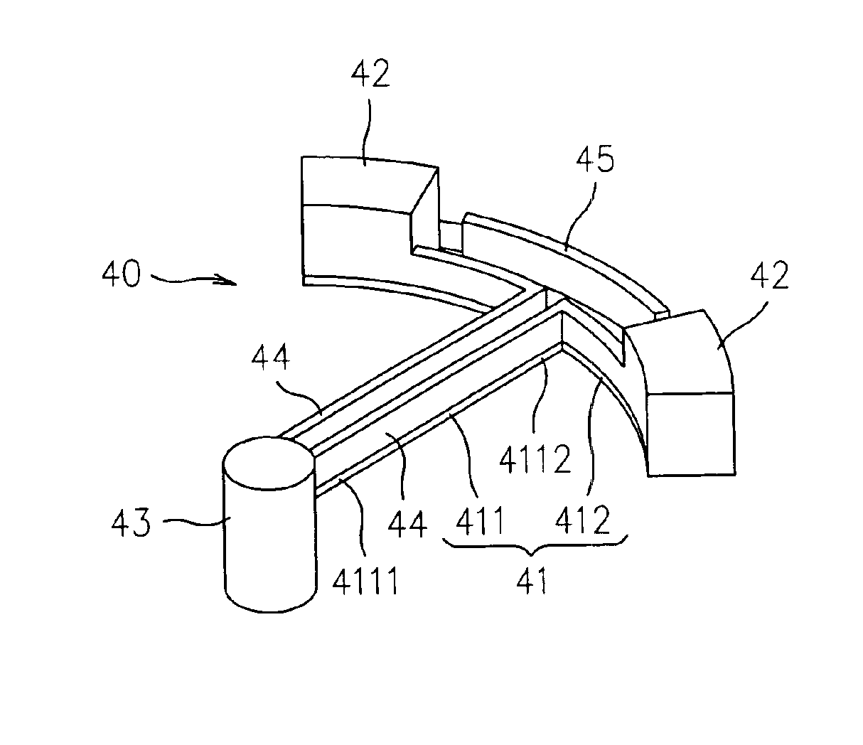
[0036]Again, please refer to FIG. 6, which shows another embodiment for the inertia sensor. The inertia sensor 40 is comprised of a suspension structure 41 and a micro-electroplating structure 42. The suspension structure 41 has an arm 411, one side 4111 of which is connected to a supporting piece 43, and another side 4112 of which is shown as suspending state and is extended horizontally to two sides to form a platform ...


PUM


Abstract

An inertia device is constructed by both suspension structure and micro-electroplating structure. The suspension structure may be manufactured by surface micromachining technique of sacrificial layer process or bulk micromachining technique incorporating with thin film process. One side of the suspension structure is arranged firmly to a supporting piece, so that another side of the suspension structure is in a suspension state. The suspension side of the suspension structure is made as micro-electroplating structure through the micro-electroplating process and functions as inertia mass for an inertia sensor. The size of the micro-electroplating structure may be changed through the micro-electroplating process, such that the inertia sensor may be adapted for sensing in different levels. Furthermore, a microstructure of high aspect ratio may be achieved by taking the advantage of a metal during the selection of a processing material, such that the objective for lateral sensing or driving signal may be fulfilled.

Description

[0001]This nonprovisional application claims priority under 35 U.S.C. § 119(a) on Patent Application No(s). 92121324 filed in TAIWAN on Aug. 5, 2003, which is(are) herein incorporated by reference.FIELD OF THE INVENTION[0002]The invention relates to an inertia sensor, and in particular, to a device with inertia mass, which size may be changed, formed upon suspension structure by micro-electroplating process.BACKGROUND OF THE INVENTION[0003]Currently, there are roughly four kinds of manufacturing techniques in Micro Electric Mechanical System (MEMS) applied for inertia sensor: surface micromachining, bulk micromachining, LIGA process, and other micromachining techniques.[0004]Wherein, the surface micromachining is to apply thin film deposition and etching technique of semiconductor process to manufacture MEMS elements on chips. As shown in FIG. 1, the steps for constructing suspension structure by surface micromachining may be classified as follows:[0005](a) Depositing isolation laye...

Claims


Application Information

Patent Timeline
Patent Type & Authority Patents(United States)
IPC IPC(8): G01P15/08
CPCG01P15/0802
Inventor CHEN, YI-RUCHANG, KAI-CHENGFANG, GUANG-CHYENGHSU, MING-HSIULIANG, PEI-FANG
Owner IND TECH RES INST
Why Eureka
Try Eureka